Video Input
Jetson AGX Xavier Series Product DG-09840-001_v2.5 | 90
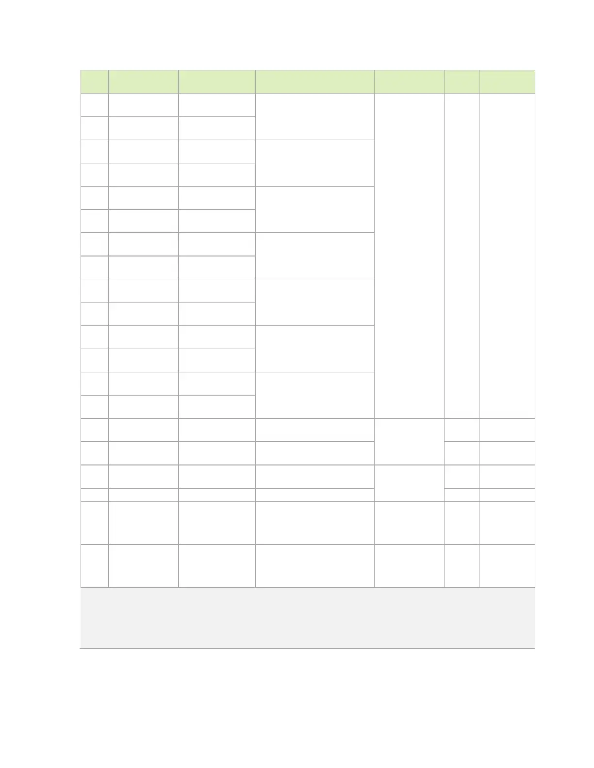
Pin # Module Pin Name SoC Signal Usage/Description
Usage on NVIDIA
Carrier Board
Direction
Pin Type
B24
NVHS0_SLVS_RX1_
N
NVHS0_RX1_N
PCIe/SLVS Receive Lane 1
connect to
device.
B25
NVHS0_SLVS_RX1_
P
NVHS0_RX1_P
C26
NVHS0_SLVS_RX2_
N
NVHS0_RX2_N
PCIe/SLVS Receive Lane 2
C27
NVHS0_SLVS_RX2_
P
NVHS0_RX2_P
A27
NVHS0_SLVS_RX3_
N
NVHS0_RX3_N
PCIe/SLVS Receive Lane 3
A26
NVHS0_SLVS_RX3_
P
NVHS0_RX3_P
D29
NVHS0_SLVS_RX4_
N
NVHS0_RX4_N
PCIe/SLVS Receive Lane 4
D28
NVHS0_SLVS_RX4_
P
NVHS0_RX4_P
B28
NVHS0_SLVS_RX5_
N
NVHS0_RX5_N
PCIe/SLVS Receive Lane 5
B29
NVHS0_SLVS_RX5_
P
NVHS0_RX5_P
C30
NVHS0_SLVS_RX6_
N
NVHS0_RX6_N
PCIe/SLVS Receive Lane 6
C31
NVHS0_SLVS_RX6_
P
NVHS0_RX6_P
A31
NVHS0_SLVS_RX7_
N
NVHS0_RX7_N
PCIe/SLVS Receive Lane 7
A30
NVHS0_SLVS_RX7_
P
NVHS0_RX7_P
C55 GPIO18 SOC_GPIO40 SLVS Horizontal sync
PCIe x16 Connector
Output
CMOS – 1.8V
(3.3V tolerant)
K56 GPIO19 SOC_GPIO43 SLVS Vertical Sync Output
CMOS – 1.8V
(3.3V tolerant)
K57
PWM01 SOC_GPIO44
SLVS Focus
40-pin Expansion
Header
Output
CMOS – 1.8V
(3.3V tolerant)
H52 GPIO27 SOC_GPIO54 SLVS Iris Output CMOS – 1.8V
D56 SPI3_MISO SPI3_MISO GPIO or SLVS XCLR
Unused but
connected to
TRST* on PCIe x16
connector
Output
CMOS – 1.8V
(3.3V tolerant)
G56 SPI3_MOSI SPI3_MOSI GPIO or SLVS XCE
Unused, but
connected to
PEX_WAKE_N on
PCIe x16 conn.
Output
CMOS – 1.8V
(3.3V tolerant)
Notes:
1. Direct lane mapping (RX[7:0] to DX[7:0] shown in the table. Reverse mapping (RX[7:0] to DX[0:7]) has also been verified.
2. The direction of the control signals in the table are for SLVS usage. If used as GPIOs, they support input or output
(bidirectional).
3. In the Type/Dir column, Output is from Jetson AGX Xavier. Input is to Jetson AGX Xavier. Bidir is for Bidirectional signals.

 Loading...