PDP-5071PU
208
1234
1234
C
D
F
A
B
E
Pin Function
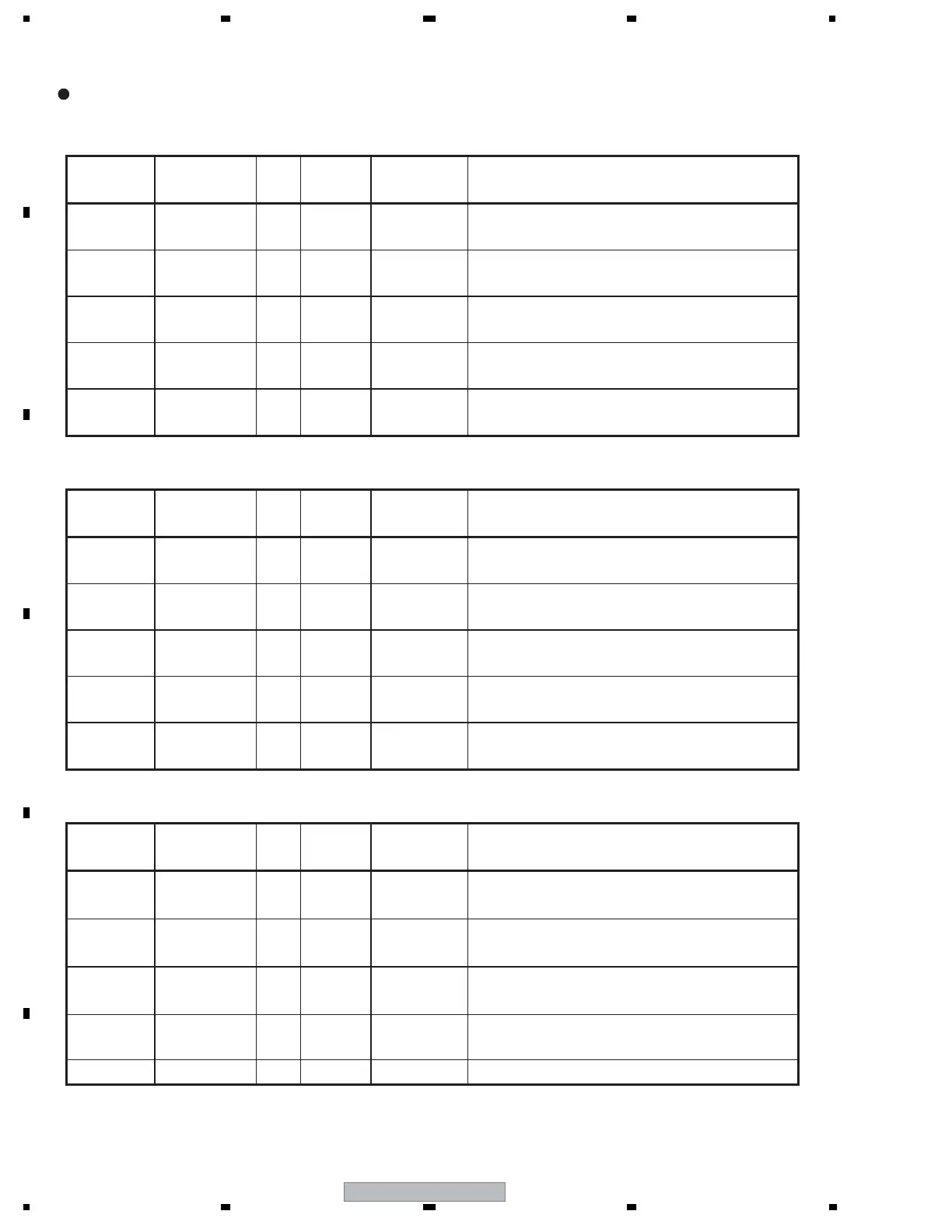
2.10 ACD3 section terminal
Acronyms Terminal number I/O Level Buffer type
PU/PD [kΩ]
Functions
ACBI 162 I Analog – ADC3 color difference component Cb signal input
Input the image signal by cutting the capacity.
ABI 164 I Analog – ADC3 RGB component B signal input
Input the image signal by cutting the capacity.
VRT3 163 I Analog – ADC3 top reference voltage
Connect to GND via a 0.1µF capacitor.
VRB3 165 I Analog – ADC3 bottom reference voltage
Connect to GND via a 0.1µF capacitor.
VCOM3 166 I Analog – ADC3 in-phase reference voltage
Connect to GND via a 0.1µF capacitor.
2.9 ACD4 section terminal
Acronyms Terminal number I/O Level Buffer type
PU/PD [kΩ]
Functions
ACRI 170 I Analog – ADC4 color difference component Cr signal input
Input the image signal by cutting the capacity.
ARI 172 I Analog – ADC3 RGB component R signal input
Input the image signal by cutting the capacity.
VCOM4 169 I Analog – ADC4 in-phase reference voltage
Connect to GND via a 0.1µF capacitor.
VRB4 173 I Analog – ADC4 bottom reference voltage
Connect to GND via a 0.1µF capacitor.
VRT4 174 I Analog – ADC4 top reference voltage
Connect to GND via a 0.1µF capacitor.
2.12 DAC section terminal
Acronyms Terminal number I/O Level Buffer type
PU/PD [kΩ]
Functions
IO-YG 62 O Analog –
Color difference component Y/RGB component G output signal.
Connect to AGNDA via a 200Ω load resistance.
IO-CR 68 O Analog –
Color difference component Cr/RGB component R output signal.
Connect to AGNDA via a 200Ω load resistance.
IO-CB 65 O Analog –
Color difference component Cb/RGB component B output signal.
Connect to AGNDA via a 200Ω load resistance.
REF 59 I Analog – External reference input pin. Supply 1.0V.
And, connect to AGNDA via a 0.1µF capacitor.
RSET 60 O Analog –
Connect to AGNDA via a 620Ω resistor for external adjustment.
 Loading...