PDP-5071PU
207
5678
56
7
8
C
D
F
A
B
E
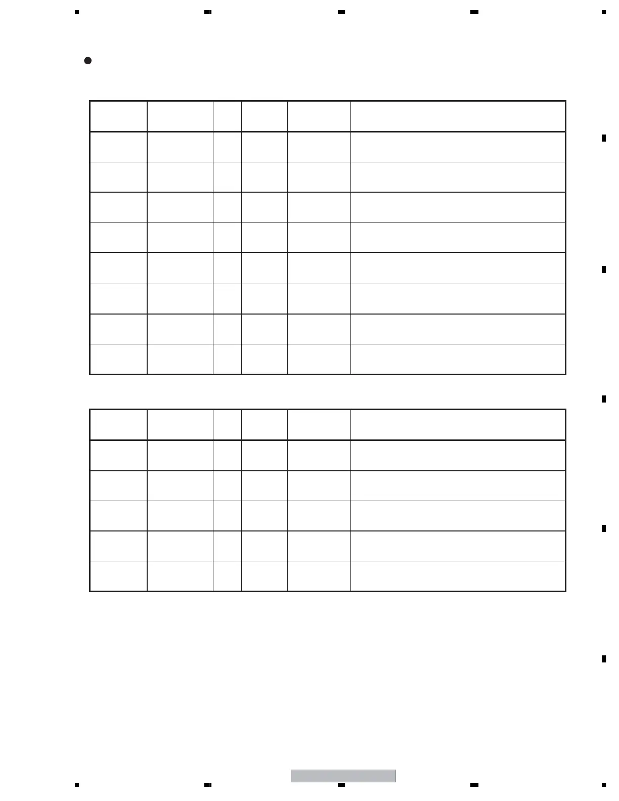
Pin Function
2.8 ADC1 section terminal
Acronyms Terminal number I/O Level Buffer type
PU/PD [kΩ]
Functions
AVI 148 I Analog – ADC1 composite/Y signal input
Input the image signal by cutting the capacity.
ASYI 150 I Analog – ADC1 composite/Y signal input
Input the image signal by cutting the capacity.
ACYI 152 I Analog – ADC1 composite/Y signal input
Input the image signal by cutting the capacity.
ACSI 154 I Analog – ADC1 composite/Y signal input
Input the image signal by cutting the capacity.
VCLY 146 O Analog – ADC1 clamp electric potential
Connect to GND via 0.1µF and 10µF capacitors.
VCOM1 147 I Analog – ADC1 in-phase reference voltage
Connect to GND via a 0.1µF capacitor.
VRB1 151 I Analog – ADC1 bottom reference voltage
Connect to GND via a 0.1µF capacitor.
VRT1 153 I Analog – ADC1 top reference voltage
Connect to GND via a 0.1µF capacitor.
2.9 ADC2 section terminal
Acronyms Terminal number I/O Level Buffer type
PU/PD [kΩ]
Functions
ASCI 158 I Analog – ADC2 separate C signal input
Input the image signal by cutting the capacity.
AGI 160 I Analog – ADC2 RGB component G signal input
Input the image signal by cutting the capacity.
VRT2 157 I Analog – ADC2 top reference voltage
Connect to GND via a 0.1µF capacitor.
VRB2 159 I Analog – ADC2 bottom reference voltage
Connect to GND via a 0.1µF capacitor.
VCOM2 161 I Analog – ADC2 in-phase reference voltage
Connect to GND via a 0.1µF capacitor.
 Loading...