Chapter 18 Debug Module (DBG) (128K)
MC9S08QE128 MCU Series Reference Manual, Rev. 2
Freescale Semiconductor 335
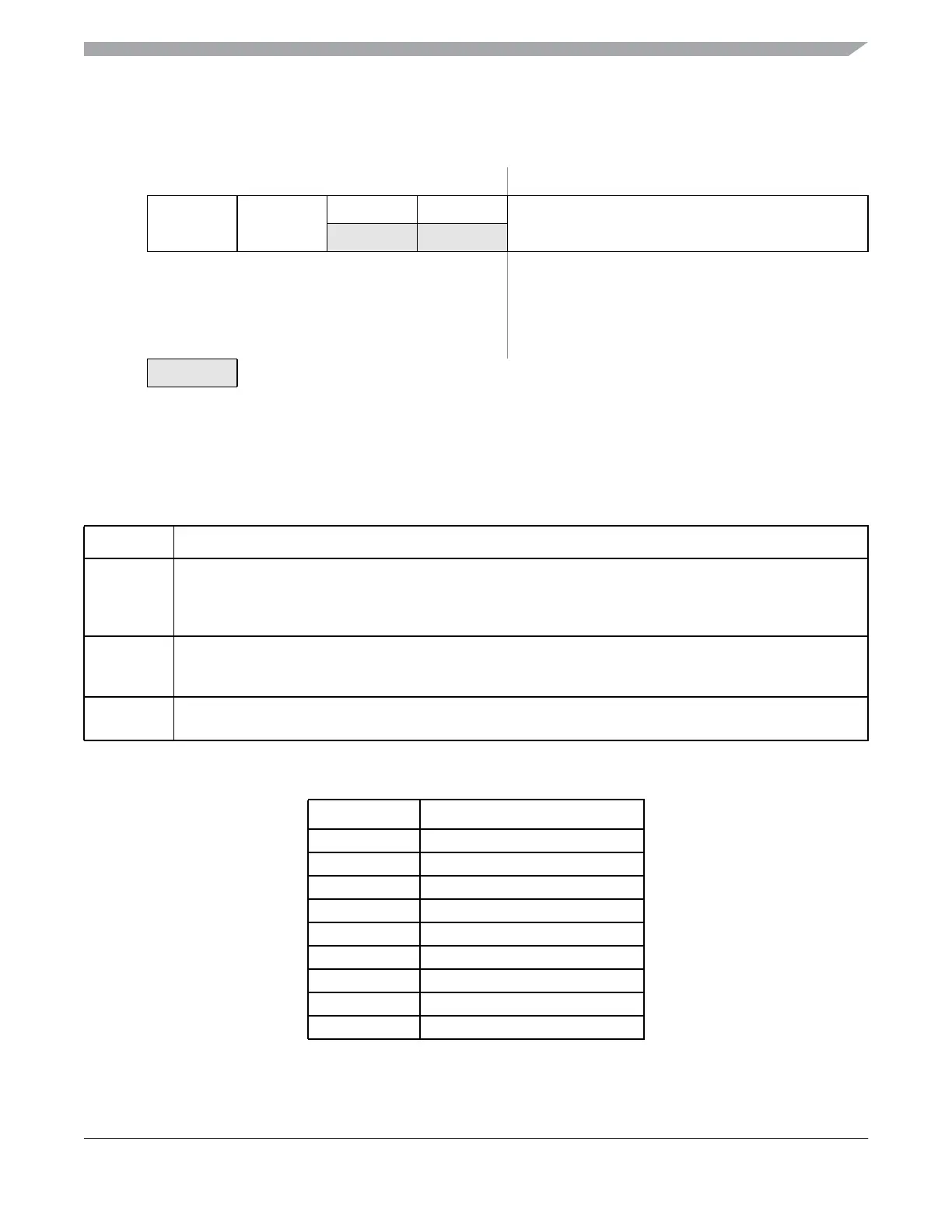
18.3.3.14 Debug Trigger Register (DBGT)
Module Base + 0x000D
76543210
R
TRGSEL BEGIN
00
TRG
W
2
POR
or non-
end-run
01000000
Reset
end-run
1
1
In the case of an end-trace to reset where DBGEN=1 and BEGIN=0, the control bits in this register do not change after reset.
2
The DBG trigger register (DBGT) can not be changed unless ARM=0.
UU00UUUU
= Unimplemented or Reserved
Figure 18-15. Debug Trigger Register (DBGT)
Table 18-16. DBGT Field Descriptions
Field Description
7
TRGSEL
Trigger Selection Bit — The TRGSEL bit controls the triggering condition for the comparators. See
Section 18.4.4, “Trigger Break Control (TBC)” for more information.
0 Trigger on any compare address access
1 Trigger if opcode at compare address is executed
6
BEGIN
Begin/End Trigger Bit — The BEGIN bit controls whether the trigger begins or ends storing of data in FIFO.
0 Trigger at end of stored data
1 Trigger before storing data
3–0
TRG
Trigger Mode Bits — The TRG bits select the trigger mode of the DBG module as shown in Table 18-17.
Table 18-17. Trigger Mode Encoding
TRG Value Meaning
0000 A Only
0001 A Or B
0010 A Then B
0011 Event Only B
0100 A Then Event Only B
0101 A And B (Full Mode)
0110 A And Not B (Full mode)
0111 Inside Range
1000 Outside Range