Chapter 4 Memory
MC9S08QE128 MCU Series Reference Manual, Rev. 2
64 Freescale Semiconductor
4.4.2.2 Linear Address Pointer Registers 2:0 (LAP2:LAP0)
The three registers, LAP2:LAP0 contain the 17-bit linear address that allows the user to access any flash
location in the extended address map. This register is used in conjunction with the data registers, linear
byte (LB), linear byte post increment (LBP) and linear word post increment (LWP). The contents of
LAP2:LAP0 will auto-increment when accessing data using the LBP and LWP registers. The contents of
LAP2:LAP0 can be increased by writing an 8-bit value to LAPAB.
4.4.2.3 Linear Word Post Increment Register (LWP)
This register is one of three data registers that the user can use to access any flash memory location in the
extended address map. When LWP is accessed the contents of LAP2:LAP0 make up the extended address
of the flash memory location to be addressed. When accessing data using LWP, the contents of
LAP2:LAP0 will increment after the read or write is complete.
76543210
R00000
XA16 XA15 XA14
W
Reset: 0 0 0 0 0 0 1 0
Figure 4-4. Program Page Register (PPAGE)
Table 4-5. Program Page Register Field Descriptions
Field Description
2:0
XA16:XA14
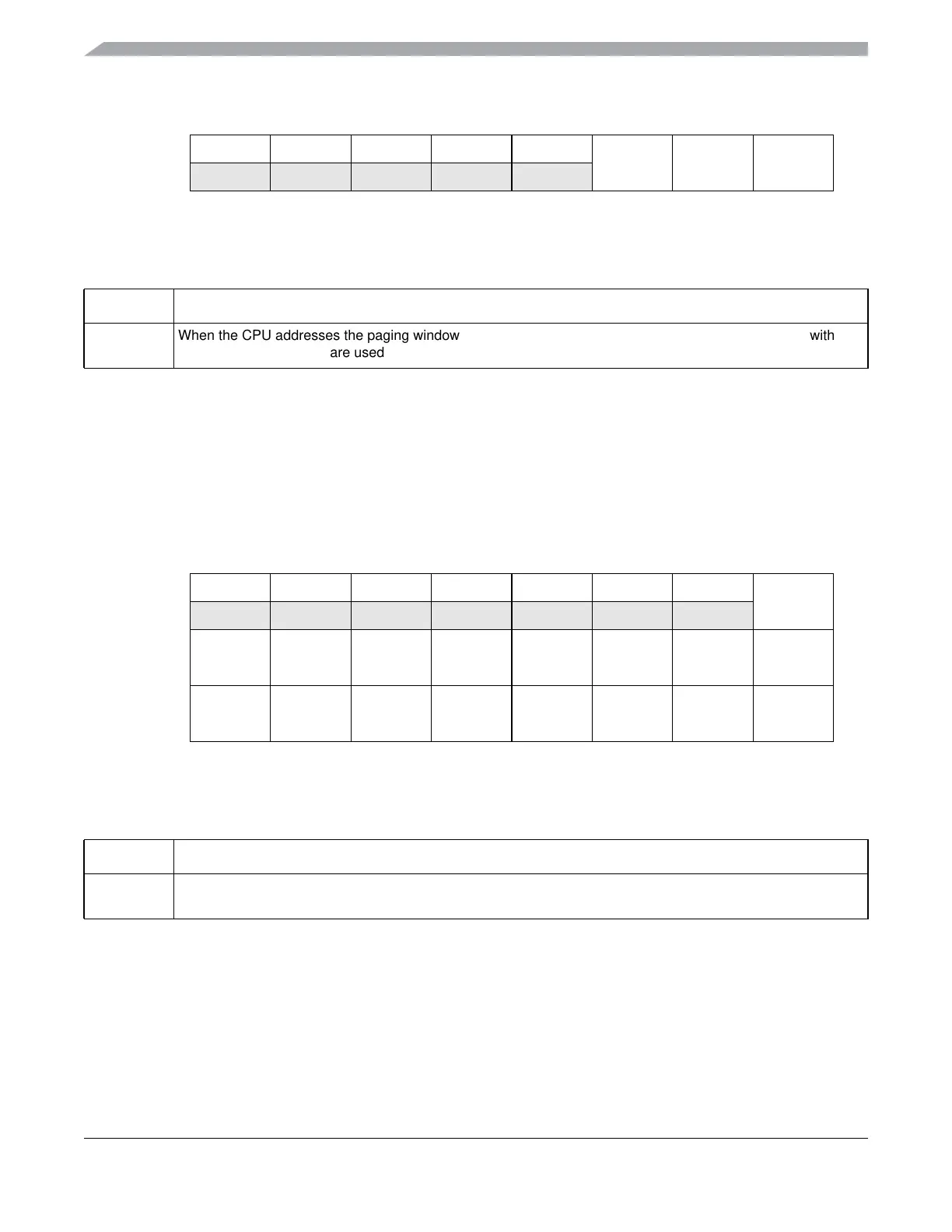
When the CPU addresses the paging window, 0x8000-0xBFFF, the value in the PPAGE register along with the
CPU addresses A13:A0 are used to create a 17-bit extended address.
76543210
R0000000
LA16
W
R
LA15 LA14 LA13 LA12 LA11 LA10 LA9 LA8
W
R
LA7 LA6 LA5 LA4 LA3 LA2 LA1 LA0
W
Reset: 0 0 0 0 0 0 0 0
Figure 4-5. Linear Address Pointer Registers 2:0 (LAP2:LAP0)
Table 4-6. Linear Address Pointer Registers 2:0 Field Descriptions
Field Description
16:0
LA21:LA0
The values in LAP2:LAP0 are used to create a 17-bit linear address pointer. The value in these registers are used
as the extended address when accessing any of the data registers LB, LBP and LWP.