Chapter 4 Memory
MC9S08QE128 MCU Series Reference Manual, Rev. 2
Freescale Semiconductor 65
Accessing LWP does the same thing as accessing LBP. The MMU register ordering of LWP followed by
LBP, allow the user to access data by words using the LDHX or STHX instructions of the LWP register.
4.4.2.4 Linear Byte Post Increment Register (LBP)
This register is one of three data registers that the user can use to access any flash memory location in the
extended address map. When LBP is accessed the contents of LAP2:LAP0 make up the extended address
of the flash memory location to be addressed. When accessing data using LBP, the contents of LAP2:LAP0
will increment after the read or write is complete.
Accessing LBP does the same thing as accessing LWP. The MMU register ordering of LWP followed by
LBP, allow the user to access data by words using the LDHX or STHX instructions with the address of the
LWP register.
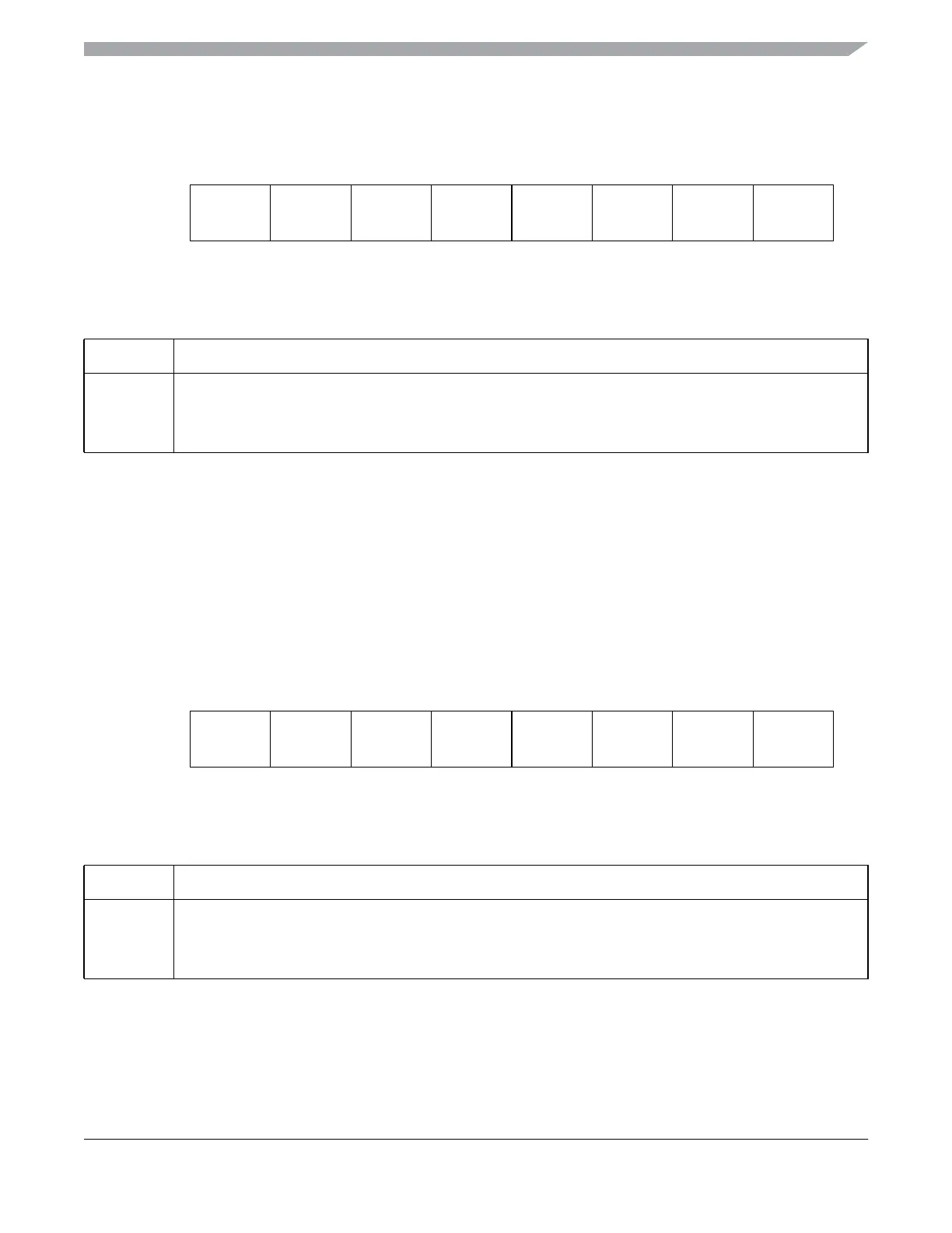
76543210
R
D7 D6 D5 D4 D3 D2 D1 D0
W
Reset: 0 0 0 0 0 0 0 0
Figure 4-6. Linear Word Post Increment Register (LWP)
Table 4-7. Linear Word Post Increment Register Field Descriptions
Field Description
7:0
D7:D0
Reads of this register will first return the data value pointed to by the linear address pointer, LAP2:LAP0 and then
will increment LAP2:LAP0. Writes to this register will first write the data value to the memory location specified
by the linear address pointer and then will increment LAP2:LAP0. Writes to this register are most commonly used
when writing to the flash block(s) during programming.
76543210
R
D7 D6 D5 D4 D3 D2 D1 D0
W
Reset: 0 0 0 0 0 0 0 0
Figure 4-7. Linear Byte Post Increment Register (LBP)
Table 4-8. Linear Byte Post Increment Register Field Descriptions
Field Description
7:0
D7:D0
Reads of this register will first return the data value pointed to by the linear address pointer, LAP2:LAP0 and then
will increment LAP2:LAP0. Writes to this register will first write the data value to the memory location specified
by the linear address pointer and then will increment LAP2:LAP0. Writes to this register are most commonly used
when writing to the flash block(s) during programming.