The pulse ourput is
an
open
NPN
emitter, and therefore
requires
a
pull-down
resistor
to
ground or to any negative
voltage. Any pull-down voltage
between ground
and
.5
volt
above the voltage on the negative
supply pin will precisely deter-
mine
the
lower level of the
pulse wave. For pull-down
voltages more negative than this,
the
lower level will
be
nearly
the negative supply pin voltage.
to finite comparator gain.
It
may
be speeded
up
considerably
by
adding hysteresis as shown in
Figure
3.
Care should
be
exer-
cised in the layout
to
prevent
stray capacitive coupling
be-
tween the pulse output and
the
PWM
input,as this can cause
comparator oscillation.
The
square
wave
output (pin
7)
from
the
GEM
3345
also
requires
a
pull down resistor to
any
negative supply greater
than
-4
volts. It provides an
output swing from nominally
1.3
uolts below the hard
sync
reference voltage to
a
level
nominally the same
as
the
hard
sync reference voltage. The
Block Diagram shows
a
con-
venient
way
of generating
a
full
swing
squaw wave from
this output.
She
current pulFed
down from
this
output should
also be limited to
a
maximum
of 3mA.
The nominal upper level of the
pulse wave is given
by:
v,,
-
Frequency
Synchronization
0.3V
-1.3K
~PLD
for
IPLD
>
The oscillator frequency may be
0.6mA,
and
Vcc
-
Q.9V
for
hard synchronized
~n
several
IPLD<
0.6mA.
where
~PLD
is
the
different ways. One
way
is to
pull down current.
A
maximum
couple positive pulses, negative
value of 3mA
for
IPLD is recorn-
~u'lses.
or
both.
into
the
hard
mended. For those
applications
which require
a
more stable, well
defined upper level, the circuits
shown in Figure
2
may
be
used.
The pulse width
of
the
pulse
output
may
be
set
from
0
to
100%
with
a
0
to
+5V
external
voltage
{VCC
=
+I
SVI
applied
to the
PWM
control input pin
[pin
5
on
the
3340
and
3345).
The fall time
of
the pulse
wave
is
slower than the rise time
due
sync
input pin pin
6
on the
3340 and
3345).
A
positive
sync
pulse will cause the triangle
wave
to
reverse directions only
during
the
rising porti~n
of
the
triangle, while
a
negattve
sync
pulse will
cause
direction reversal
only during the falling portion.
The resulting
waveforms
are
shown in Figure
I.
and
provide
a
wider variety
of
synchronized
sounds than possible through
conventionaFly synchronized
oscillators. Simple capacitive
coupling as shown in the
Black
Diagrams
allows hard synchron-
ization on
both
the
rising and
falling edge
of
a
rectangbe wave.
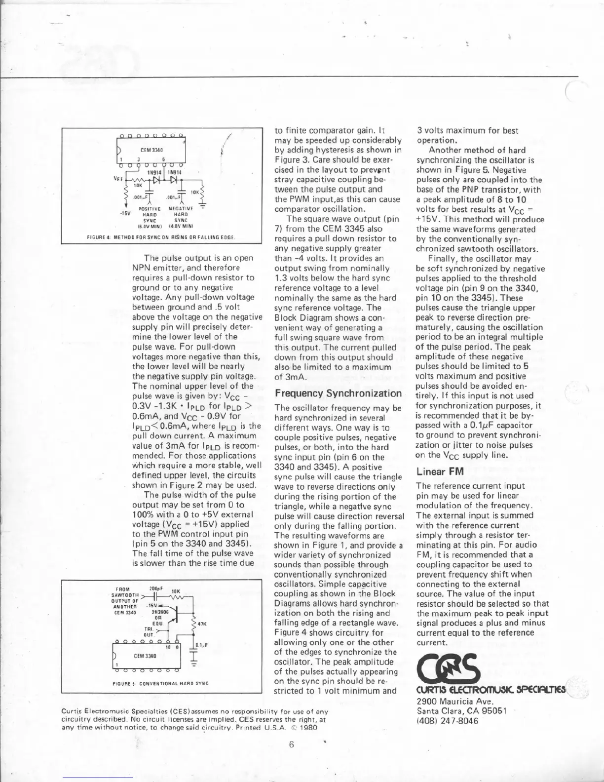
Figure
4
shows circuitry for
allowing only one or the other
of the edges
to
synchronize the
oscillator. The
peak
amplitude
of
the
pulses actually appearing
on
the sync pin should
be
re-
stricted to
il
volt minimum and
Curt~s
Electromusrc
Specraltles
(CESlassumes
no
respons~b~l~ty
for
use
of
any
clrcultry
descrtbed
No
clrcult
licenses
are
~mplied
CES
reserves the rlght,
at
any
time
w~thout
norm,
to
change
said
~lrcuitrv Pr~nted
U
5.A
C
6980
3
volts
maximum
for
best
operation.
Another
method
of hard
synchronizing the
oscilrator is
shown
in
Figure
5.
Negative
pulses only are coupled into the
base
of
the
PNP
transistor, with
a
peak
amplitude of
&
to
10
volts for best results
at
VcC
=
+T5V.
This method
will
pr~duce
the
same
waveforms generated
by
the
conventionally
syn-
chronized sawtooth oscillators.
Finally.
the
oscillator
may
be soft synchronized
by
negative
pulses applied to
the
threshold
voltage
pin
(pin
9
on
the
3340,
pin 10 on the
33451.
These
pulses cause the triangle upper
peak
to
reverse direction
pre-
maturefy, causing the oscillation
period
to
be
an
integral multiple
of
the pulse period. The peak
amplitude of these negative
pulses should
be
limited to
5
volts maximum and positive
pulses should
be
avoided en-
tirely. If this
input
is not used
for synchronization purposes, it
is
recommended
that
it be
by-
passed with
a
Q.1pF
capacitor
to
ground to prevent synchroni-
zation
or
jitter ta noise pulses
an
the
Vcc
supply line.
Linear
FM
The reference current input
pin may be used for linear
modulation
of
the frequency.
The external input
is
summed
with the reference current
simply
through
a
resistor ter-
minating at this pin.
For
audio
FM,
it
is rectlmmended that
a
coupling capacitor be used to
prevent frequency shift when
connecting to the external
source. The value
of
the input
resistor should
be
selected so that
the
maximum
peak
to
peak
input
signal produces
a
plus and minus
current equal
te
the reference
current.
2900
Maur~cia
Ave.
Santa
Clara,
CA
95051
I4081
247-8046