bit_period is a three bit gray counter, incrementing every clock cycle (around 13 ns).
Thus, it is only possible to execute one write command every eight clock cycles, which
takes about 110 ns. Of course, if the customer interface connected will issue com‐
mands significantly slower, and it is known that the write flag will be active for a time
greater than 110 ns, bit_period doesn’t need to be monitored. It is only needed
when aiming for the most rapid interfacing.
9.5 Register assignment
The address assignment of the registers depends on the bigend control signal and
likewise on the dsl_8n16 control signal for 16 bit wide parallel bus interfaces.
NOTE
It should be noted that only 8 bit addressing is available when using the SPI interface
block.
When using the parallel bus interface block (EMIFA) with 16 bit addressing, the register
addresses must be assigned to the dsl_a and dsl_ba signals as follows:
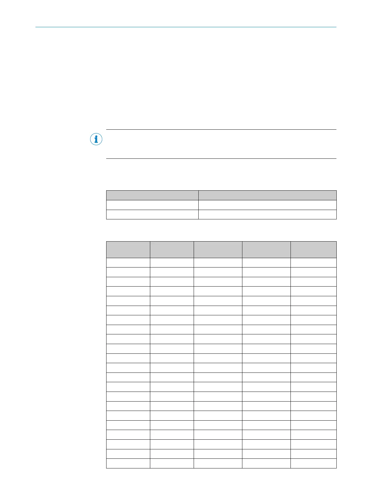
Table 196: Parallel bus register address assignment
Signal Register address
dsl_a[5:0] Bit 6:1
dsl_ba Bit 0
The table below specifies the relevant address assignment.
Table 197: Address assignment for the DSL Master
Designation 8 bit, Big-Endian 8 bit, Little-Endian 16 bit, Big-Endian 16 bit, Little-
Endian
SYS_CTRL 00h 03h 00h (15:8) 02h (15:8)
SYNC_CTRL 01h 02h 00h ( 7:0) 02h ( 7:0)
MASTER_QM 03h 00h 02h ( 7:0) 00h ( 7:0)
EVENT_H 04h 07h 04h (15:8) 06h (15:8)
EVENT_L 05h 06h 04h ( 7:0) 06h ( 7:0)
MASK_H 06h 05h 06h (15:8) 04h (15:8)
MASK_L 07h 04h 06h ( 7:0) 04h ( 7:0)
MASK_SUM 08h 0Bh 08h (15:8) 0Ah (15:8)
EDGES 09h 0Ah 08h ( 7:0) 0Ah ( 7:0)
DELAY 0Ah 09h 0Ah (15:8) 08h (15:8)
VERSION 0Bh 08h 0Ah ( 7:0) 08h ( 7:0)
ENC_ID2 0Dh 0Eh 0Ch ( 7:0) 0Eh ( 7:0)
ENC_ID1 0Eh 0Dh 0Eh (15:8) 0Ch (15:8)
ENC_ID0 0Fh 0Ch 0Eh ( 7:0) 0Ch ( 7:0)
POS4 10h 17h 10h (15:8) 16h (15:8)
POS3 11h 13h 10h ( 7:0) 12h (15:8)
POS2 12h 12h 12h (15:8) 12h ( 7:0)
POS1 13h 11h 12h ( 7:0) 10h (15:8)
POS0 14h 10h 14h (15:8) 10h ( 7:0)
VEL2 15h 16h 14h ( 7:0) 16h ( 7:0)
VEL1 16h 15h 16h (15:8) 14h (15:8)
VEL0 17h 14h 16h ( 7:0) 14h ( 7:0)
9 FPGA IP-CORE
150
T E C H N I C A L I N F O R M A T I O N | HIPERFACE DSL
®
8017595/ZTW6/2018-01-15 | SICK
Subject to change without notice
 Loading...