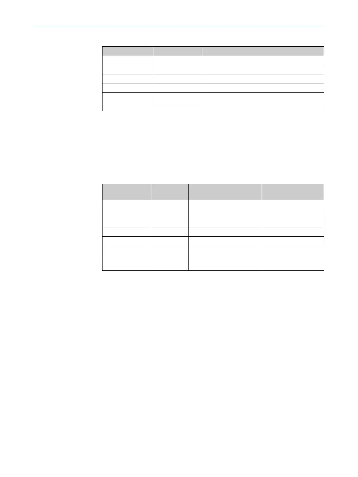
Table 194: Additional parallel interface block signals
Interfaces signal Value Function
dsl_freeze Use for consistent multi-byte access
0 Multi-byte registers are refreshed
1 Multi-byte registers are frozen
dsl_8n16 Use for selection of the data bus width
0 16 bit width
1 8 bit width
Also, because of the selection of bigend, the register assignment of the DSL Master
should be taken into account.
9.4 Basic interface specification
If a fast connection of the IP-Core registers is needed the user can develop an own
interface block directly connected to the basic interface. The following signals are avail‐
able for interfacing the IP Core directly:
Table 195: Direct interfacing signals
Pin name IP Core signal
type
Function Note
hostd_a(6:0) input Register block address bus
hostd_di(7:0) input Data in bus interface to core
hostd_do(7:0) output Data out bus core to interface
hostd_r input Read access identifier
hostd_w input Write access identifier
hostd_f input Register block freeze indicator
bit_period(2:0) output Internal state machine timing aux_signals (4:2) top
level output
9.4.1 General information
The main signals for accessing the basic interface are the address bus (hostd_a), the
data in (hostd_di) and data out (hostd_do) lines as well as their respective read and
write flags (hostd_r and hostd_w). Apart from these access signals, there are two
other important signals:
1 The register freeze flag (hostd_f)
This flag controls the updating of multi-byte registers inside the IP Core. When it is
raised to ‘1’, no further updates are done for those multi-byte registers. Update
values are stored separately, but will not be available in their corresponding regis‐
ters until the freeze flag drops to ‘0’ again. This procedure should be used when‐
ever a multi-byte register is read, to avoid updates in between read operations of a
single set of data.
2 The internal timing reference (bit_period)
Some registers care for being read by the user, and there is a specific timing when
the data from the data in line is actually written to the register on which the write
command is issued. Therefore, when implementing the fastest possible communi‐
cations, the user needs to be aware of these timings.
9 FPGA IP-CORE
148
T E C H N I C A L I N F O R M A T I O N | HIPERFACE DSL
®
8017595/ZTW6/2018-01-15 | SICK
Subject to change without notice
 Loading...