- 68 -
No.EX##-OMY0004
Parameter setting for the commissioning mode
Fixed parameter setting during the commissioning mode
Table 10-32 Fixed Parameters
Sensor power supply (Clock configuration)
1oo1 evaluation (Input N, N+4)
Power source for cross-circuit detection
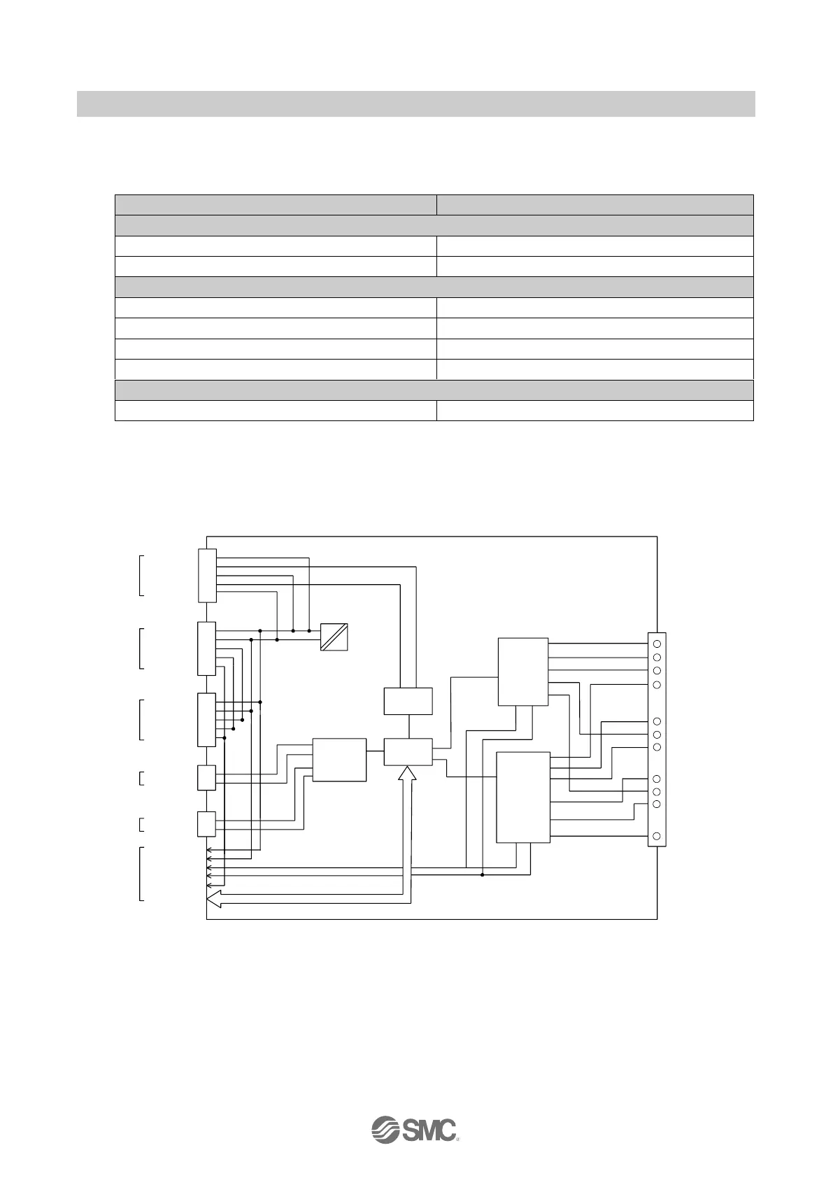
10.12. Block diagram
The following figure shows the block diagram of each SI Unit.
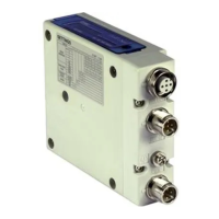
Fig. 10-10 Block diagram of the EX245-FPS1
TX
RX
Bus
Module
interface
24 V (US1)
0 V ( US1)
0 V (M OUT)
24 V (P OUT)
FE
Bus
Internal
Logic circuit
DC / DC
0 V (M OUT)
1
24V (ZONE OUT 2)
11
2
3
・ ・ ・ ・
Standard
Output circuit
Push Pull connector (SCRJ)
①
②
Power
Push Pull connector (24 Volt)
0V(US1)
24V(US1)
24V(US2)
0V(US2)
FE
④
②
⑤
①
③
TX
RX
Bus
②
①
ERTEC200
Push Pull connector (SCRJ)
Port1 (x1)
Port2 (x2)
Power
Push Pull connector (24 Volt)
0V(US1)
24V(US1)
24V(US2)
0V(US2)
FE
④
②
⑤
①
③
④
②
⑤
①
③
4 x M12, 5 way, Sockets
DI(n+1)
24V(UT1)
0V
DI(n)
24V(UT2)
Sensor
interface
Safe
Input circuit
Safe
Output circuit
4
0 V (M OUT)
24V (ZONE OUT 1)
OUT [0]
OUT [7]
12
13
OUT [8]
・ ・ ・ ・
24V (ZONE OUT 3)
20
OUT [15]
21
22
OUT [16]
・ ・ ・ ・
29
OUT [23]
 Loading...