5959
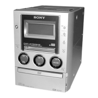
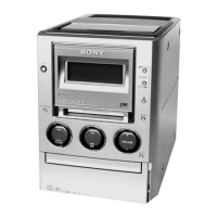
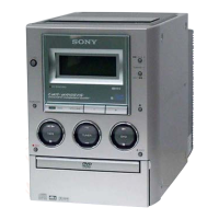
HCD-M700
THIS NOTE IS COMMON FOR PRINTED WIRING
BOARDS AND SCHEMATIC DIAGRAMS.
(In addition to this, the necessary note is printed
in each block.)
For schematic diagrams.
Note:
• All capacitors are in µF unless otherwise noted. pF: µµF
50 WV or less are not indicated except for electrolytics
and tantalums.
• All resistors are in Ω and
1
/
4
W or less unless otherwise
specified.
•
f
: internal component.
• 2 : nonflammable resistor.
• 1 : fusible resistor.
• C : panel designation.
For printed wiring boards.
Note:
• X : parts extracted from the component side.
• Y : parts extracted from the conductor side.
•
a
: Through hole.
• : Pattern from the side which enables seeing.
• A : B+ Line.
• B : B– Line.
• H : adjustment for repair.
•Voltages and waveforms are dc with respect to ground
under no-signal (detuned) conditions.
•Voltages are taken with a VOM (Input impedance 10 MΩ).
Voltage variations may be noted due to normal produc-
tion tolerances.
•
∗
: Impossible to measure
•Waveforms are taken with a oscilloscope.
Voltage variations may be noted due to normal produc-
tion tolerances.
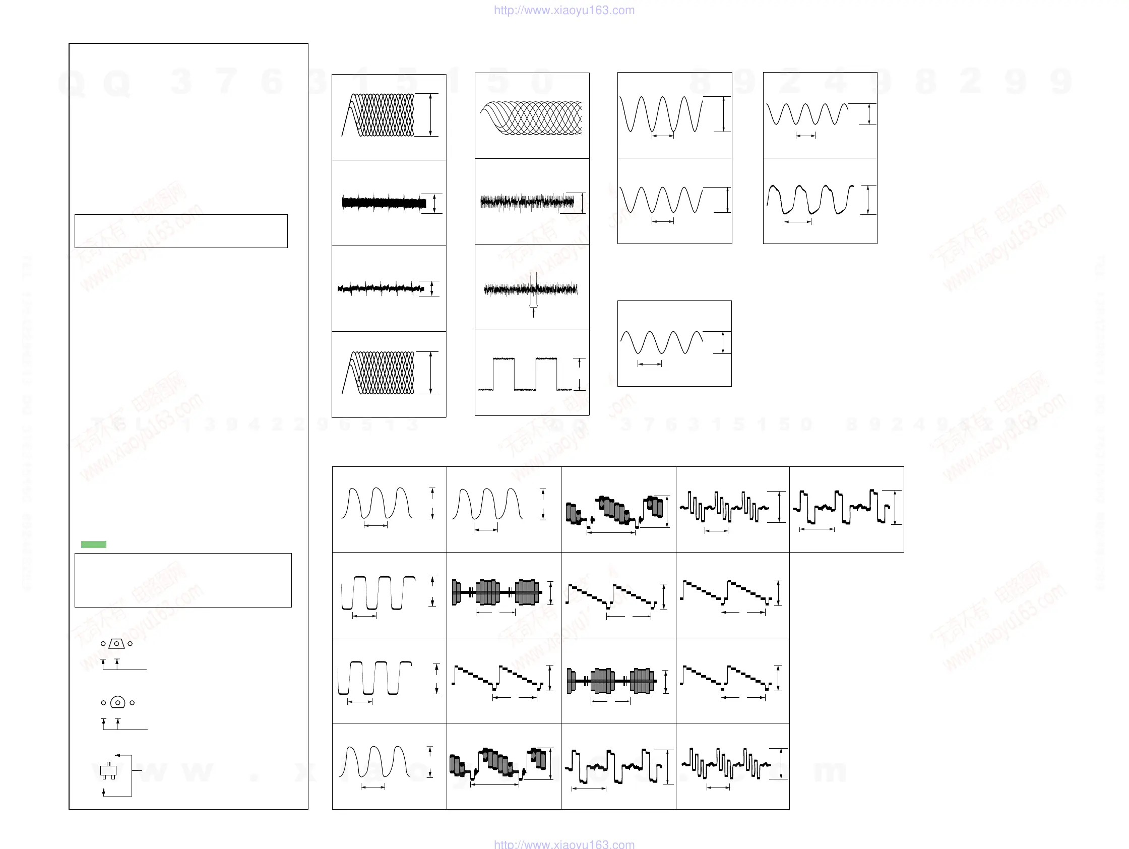
• Circled numbers refer to waveforms.
• Signal path.
F : FM
J : DVD
c : DVD DIGITAL
p : PB (MD)
l : REC (MD)
I : DIGITAL AUDIO
g : VIDEO
•Abbreviation
HK : Hong Kong model
Note: The components identified by mark 0 or dotted line
with mark 0 are critical for safety.
Replace only with part number specified.
• Indication of transistor
B
These are omitted.
CE
B
These are omitted.
CE
C
B
These are omitted.
E
Q
• Waveforms
– BD Board –
1 IC101 ek (RF)
2 IC101 ef (FE) (Play mode)
4 IC151 o; (FS4)
3 IC101 wh (TE) (Play mode)
1.3 Vp-p
0.2 Vp-p
1.6 Vp-p
during track jump
3.5 Vp-p
176.4 kHz
– DIGITAL Board –
1 IC701 qf (XTALOUT)
2 IC721 qd (XOUT)
81 ns
3.9 Vp-p
1 V/DIV, 40 ns/DIV
100 ns
3.4 Vp-p
1 V/DIV, 40 ns/DIV
– RF-240 Board –
1 IC001 2 (RFIN)
2 IC001 ra (TE)
4 IC001 tl (SIGO)
3 IC001 rs (FE)
0.1 V/DIV, 1 ms/DIV
0.2 V/DIV, 100 ns/DIV
0.5 V/DIV, 100 ns/DIV
0.5 V/DIV, 1 ms/DIV
0.72 Vp-p
0.5 Vp-p
0.3 Vp-p
1.4 Vp-p
– CONTROL Board –
1 IC306 qd (XOUT)
2 IC306 qa (XCOUT)
3.4 Vp-p
30.5
µ
s
1 V/DIV, 10
µ
s/DIV
62.5 ns
2 Vp-p
1 V/DIV, 40 ns/DIV
– TC Board –
12
µ
s
12.7 Vp-p
5 V/DIV, 4
µ
s/DIV
1
Q401 collector (TAPE REC)
1 IC102 8 (XTO)
2 IC102 9 (512FS6CH)
6 IC701 2 (INA)
5 IC103 td (X1)
3 IC102 qd (33MAVD)
29.5 ns
37 ns
37 ns
60.6 ns
44 ns
1 V/DIV, 10 ns/DIV
1 V/DIV, 20 ns/DIV
1 V/DIV, 10 ns/DIV
1 V/DIV, 10 ns/DIV
1 V/DIV, 10 ns/DIV
200 mV/DIV, 20
µ
s/DIV
4.5 Vp-p
4.1 Vp-p
4.2 Vp-p
4 IC102 3 (27MAVD)
4.7 Vp-p
3.9 Vp-p
0.7 Vp-p
H
7 IC701 4 (INB)
8 IC701 7 (INC)
0 IC701 qs (OUT B2)
qs IC702 2 (INA)
qa IC701 qg (OUT A1)
9 IC701 9 (OUT C2)
500 mV/DIV, 20
µ
s/DIV
500 mV/DIV, 20
µ
s/DIV
200 mV/DIV, 20
µ
s/DIV
500 mV/DIV, 20
µ
s/DIV
500 mV/DIV, 20
µ
s/DIV
200 mV/DIV, 20
µ
s/DIV
H
1.0 Vp-p
H
1.3 Vp-p
H
2.6 Vp-p
H
2.0 Vp-p
H
1.3 Vp-p
H
0.8 Vp-p
0.8 Vp-p
H
qd IC702 4 (INB)
qf IC702 7 (INC)
qh IC702 qs (OUT B2)
qj IC702 qg (OUT A1)
qg IC702 9 (OUT C2)
500 mV/DIV, 20
µ
s/DIV
500 mV/DIV, 20
µ
s/DIV
200 mV/DIV, 20
µ
s/DIV
200 mV/DIV, 20
µ
s/DIV
500 mV/DIV, 20
µ
s/DIV
1.0 Vp-p
H
2.0 Vp-p
H
1.6 Vp-p
H
H
1.6 Vp-p
– DVD Board –
Caution:
Pattern face side: Parts on the pattern face side seen from
(SIDE B) the pattern face are indicated.
Parts face side: Parts on the parts face side seen from
(SIDE A) the parts face are indicated.
w
w
w
.
x
i
a
o
y
u
1
6
3
.
c
o
m
Q
Q
3
7
6
3
1
5
1
5
0
9
9
2
8
9
4
2
9
8
T
E
L
1
3
9
4
2
2
9
6
5
1
3
9
9
2
8
9
4
2
9
8
0
5
1
5
1
3
6
7
3
Q
Q
TEL 13942296513 QQ 376315150 892498299
TEL 13942296513 QQ 376315150 892498299
http://www.xiaoyu163.com
http://www.xiaoyu163.com