55
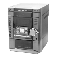
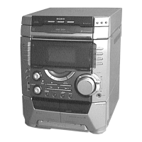
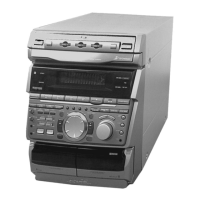
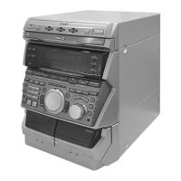
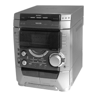
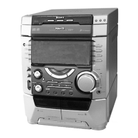
HCD-VX888
6-32. IC PIN FUNCTION DESCRIPTION
• MAIN BOARD IC501 M30620MCA-A95FP (SYSTEM CONTROLLER)
Pin No. Pin Name I/O Description
1
AUDIO OUT
ON/OFF
O
Audio output on/off control signal output to the Audio SWITCH (IC401)
“H”: ON, “L” OFF
2
STEREO I Stereo detection signal input from the LA1845 (IC11) “L”: Stereo in
3
TUNED
I
Tuning detection signal input from the LA1845 (IC11) “L”: Tuned in
4
SIRCS
I
Remote commander receiver signal input terminal
5 SUR1 O
Surround control signal output to the LA2615 (IC103)
6 SUR2 O
Surround control signal output to the LA2615 (IC103)
7
SUR3
O
Surround control signal output to the LA2615 (IC103)
8
GND — Ground terminal
9 GND
— Ground terminal
10
XC IN I Sub system clock input terminal (32.768 kHz)
11
XC OUT O Sub system clock output terminal (32.768 kHz)
12
RESET I System reset signal input from the reset signal generator (IC502) “L”: reset
13 X-OUT
O Main system clock output terminal (16 MHz)
14 VSS
— Ground terminal
15 X-IN
I Main system clock input terminal (16 MHz)
16 VCC
— Power supply terminal (+5V)
17
NMI I For pull up terminal (connected to Ever +5V)
18 RDS-INT
I RDS interrupt signal input terminal Not used (fixed at “L”)
19 SCOR
I Subcode sync (S0+S1) detection signal input terminal Not used (fixed at “L”)
20 RDS-DATA I
RDS data signal input terminal Not used (fixed at “L”)
21 ST-MUTE O
Muting on/off control signal output to the LA1845 (IC11)
22 ST-CE O
PLL chip enable signal output to the FM/AM PLL (IC51)
23 ST-DOUT
O PLL serial data output to the FM/AM PLL (IC51)
24 BU-PWM3
O RF data control signal output terminal Not used (open)
25
ST-DIN I PLL serial data input from the FM/AM PLL (IC51)
26 BU-PWM2
O Tracking error control signal output terminal Not used (open)
27
ST-CLK
O
PLL serial data transfer clock signal output to the FM/AM PLL (IC51)
28
BU-PWM1 O Focus error control signal output terminal Not used (open)
29
IIC-CLK I/O Shift clock signal input/output for the IIC bus
30
IIC-DATA I/O Data input/output terminal for the IIC bus
31
TXD1 O Not used (open)
32
SQ-DATA I Subcode Q data input terminal Not used (fixed at “L”)
33
SQ-CLK O Subcode Q data reading clock signal output terminal Not used (open)
34
SENS I Internal status detection monitor input terminal Not used (fixed at “L”)
35
CD-DATA O Serial data output terminal Not used (open)
36
NC — Not used (fixed at “L”)
37
CD-CLK O Serial clock signal output terminal Not used (open)
38
CD-POWER O CD power on/off control signal output “L”: on, “H”: off
39 CLOCK-OUT
O Clock signal output terminal Not used (open)
40
HOLD O Automatic power control hold signal output terminal Not used (open)
41
M-RESET O Micom reset signal output to the liquid crystal display driver (IC601) “L”: reset
42
XLT O Serial data latch pulse output terminal Not used (open)
43
XRST O CD reset signal output to the CXD3017Q (IC101) and BA5974FM (IC102) “L”: reset
44
LOAD-IN O Turn motor control signal output to the BA6956AN (IC701)
w
w
w
.
x
i
a
o
y
u
1
6
3
.
c
o
m
Q
Q
3
7
6
3
1
5
1
5
0
9
9
2
8
9
4
2
9
8
T
E
L
1
3
9
4
2
2
9
6
5
1
3
9
9
2
8
9
4
2
9
8
0
5
1
5
1
3
6
7
3
Q
Q
TEL 13942296513 QQ 376315150 892498299
TEL 13942296513 QQ 376315150 892498299
http://www.xiaoyu163.com
http://www.xiaoyu163.com