4242
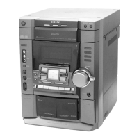
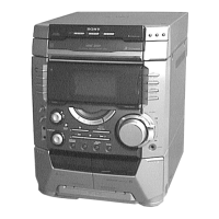
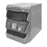
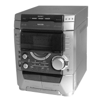
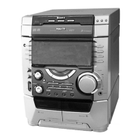
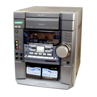
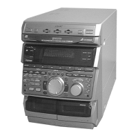
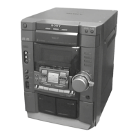
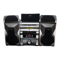
HCD-VX888
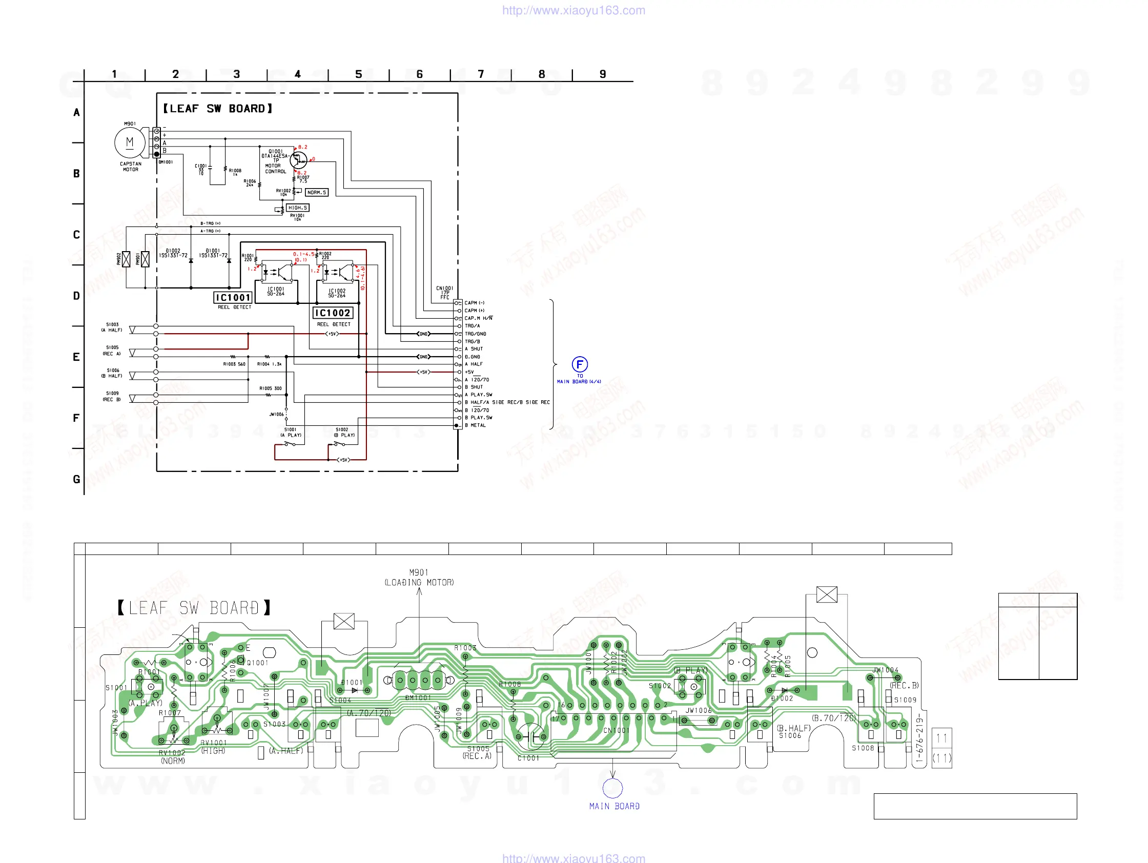
6-22. SCHEMATIC DIAGRAM – LEAF SW Board –
(Page 33)
• Voltages are dc with respect to ground under no-signal
conditions.
no mark : TAPE PLAY
( ) : TAPE REC
6-23. PRINTED WIRING BOARDS – LEAF SW Board – • See page 27 for Circuit Boards Location.
There are a few cases that the part printed on
this diagram isn’t mounted in this model.
PM901
PM902
F
CN304
IC1001
IC1002
A
B
C
D
1 2 3 4 5 6 7 8 9 10 11 12
(Page 34)
• Semiconductor
Location
Ref. No. Location
D1001 B-4
D1002 B-10
IC1001 B-2
IC1002 B-10
Q1001 B-3
w
w
w
.
x
i
a
o
y
u
1
6
3
.
c
o
m
Q
Q
3
7
6
3
1
5
1
5
0
9
9
2
8
9
4
2
9
8
T
E
L
1
3
9
4
2
2
9
6
5
1
3
9
9
2
8
9
4
2
9
8
0
5
1
5
1
3
6
7
3
Q
Q
TEL 13942296513 QQ 376315150 892498299
TEL 13942296513 QQ 376315150 892498299
http://www.xiaoyu163.com
http://www.xiaoyu163.com