ABCDE F
G
HIJKLMN
1
2
3
4
5
6
7
8
9
10
11
- 55 -
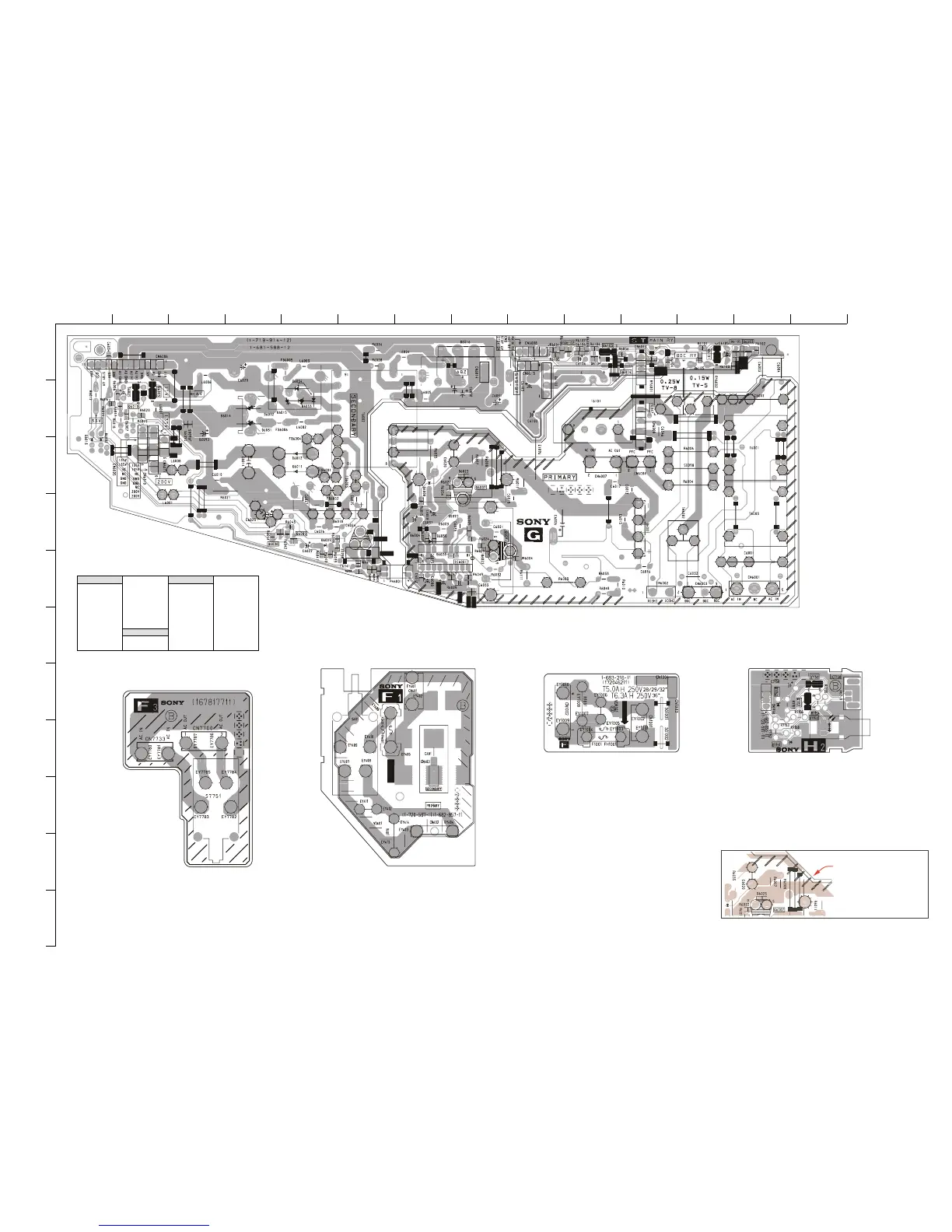
~ G Board Semiconductor Location Table ~
~ G Printed Wiring Board Conductor side ~
EDOID
5106D2-E
ROTSISNART
2016Q1-J
2006D3-A3206D3-H3006Q1-M3016Q1-J
3006D4-G0306D4-G5006Q2-B5016Q1-L
4006D4-G1306D2-D6006Q4-H
8006D3-G2306D2-D7006Q3-H
9006D4-E3306D2-E8006Q4-D
0106D4-E4306D2-E9006Q4-E
1106D3-E
CI
0106Q2-B
2106D3-E1006CI5-G4106Q2-J
3106D3-A1016Q1-L
Note :
Portions of the circuit contained within
the marked areas as shown have high
voltages present. Use care to prevent
electric shock during inspection or repair.
An Isolation Transformer must be used
during any Service work to avoid possible
shock hazard due to live chassis. The
chassis of this receiver is directly
connected to the power line.
~ F3 Printed Wiring Board Conductor side ~
~ F1 Printed Wiring Board Conductor side ~
~ H2 Printed Wiring Board Conductor side ~
~ F Printed Wiring Board Conductor side ~