76
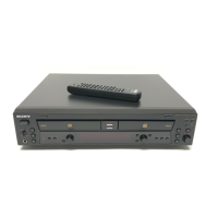
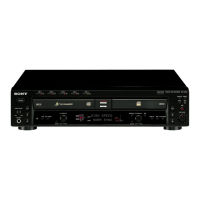
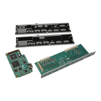
RCD-W10
• IC101 AK8567 S/H & MATRIX, MPX (CDR Board)
Pin No.
1
2
3
4
5
6
7
8
9
10
11
12
13
14
15
16
17
18
19
20
21
22
23
24
25
26
27
28
29
30
31
32
33
34
35
36
37
38
39
40
41
42
43
44
45
46
47
48
49
50
I/O
—
O
O
O
O
O
O
I
O
O
O
I
I/O
O
O
—
I
I
I/O
O
I
I
I/O
O
—
—
O
I
I
O
O
O
O
O
—
I
I
I
O
O
O
O
O
O
O
O
O
I
I
—
Pin Name
AVDD3
BCENT
PHBETA
BHBETA
PHBTC
BHBTC
MPP
TEIN
TE
FE
SBAD
TZCLVL
VREF
AGND1
BIAS
VSS
FVREF
FPDO
RREF
VRDC
VRDCN
VRDCN2
WREF
WDAO
AVDD2
AV SS2
VWDC
VWDCN2
VWDCN
ATFM
AGC1C
AGC2C
AGC3C
AGND2
VSS
SGAINDN
GAINUP
AGCON
ATFG
XTOR
XTAND
TZC
RECD2
RECD1
RC
DFCT
MIRR
MCLK1
MCLK2
DVSS
Description
Power supply (analog)
Center signal output
β signal top level signal output
β signal bottom level signal output
Extrenal capacitor teminal for PHBETA droop rate setting
Extrenal capacitor teminal for BHBETA droop rate setting
Main push-pull signal output Not used (open)
Tracking signal processing input
Tracking error signal output
Focus error signal output
SBAD signal output Not used (open)
Tracking zero cross comparate level input
Decoupling teminal for internal reference voltage / internal reference voltage input terminal
Decoupling teminal for internal reference voltage
Bias resistor connection terminal BIAS = 4.7kΩ
Ground terminal (analog)
APC reference voltage input terminal
Laser monitor voltage input
Power setting voltage input for read APC / internal DAC setting voltage output
Read laser driver control signal output
Read laser driver control amplifier (-) teminal
Read laser driver time constant setting terminal
Power setting voltage input for write APC / internal DAC setting voltage output
Power setting internal DAC voltage output for write APC Not used (open)
Power supply (analog)
Ground terminal (analog)
Write laser driver control signal output
Write laser driver time constant setting terminal
Write laser driver control amplifier (-) teminal
Wobble signal output
External capacitor terminal for AGC response speed setting
External capacitor terminal for AGC response speed setting
External capacitor terminal for AGC response speed setting
Decoupling teminal for internal reference voltage
Ground terminal (analog)
Gain selection signal input
CD-RW selection control signal input
Wobble AGC enable signal input “H” : AGC ON, “L” : AGC reset
ATIP FG signal output (Wobble signal after formation of 2 values)
Tracking amplitude detection signal output
Tracking failure detection signal output
Tracking zero cross detection signal output
Recorded block detection signal output 2 “H” : recorded block, “L” : unrecorded block
Recorded block detection signal output 1 “H” : recorded block, “L” : unrecorded block
RC signal output
DFCT signal output
MIRR signal output
Main clock input 1 (sine wave input) 34.5744MHz
Main clock input 2 (sine wave input) fixed at “L”
Ground terminal (digital)
 Loading...