77
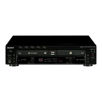
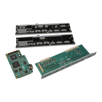
RCD-W10
Pin No.
51
52
53
54
55
56
57
58
59
60
61
62
63
64
65
66
67
68
69
70
71
72
73
74
75
76
77
78
79
80
81
82
83
84
85
86
87
88
89
90
91
92
93
94
95
96
97
98
99
100
I/O
—
O
O
I
I
I
I
I
I
I
I
I
I
I
I
I
I
I
—
O
O
O
I
O
—
—
O
O
—
O
—
I
I
I
O
I
I
O
O
—
I
I
I
I
I
I
I
I
I
—
Pin Name
DVDD
FOK
RZC
MPDSH
SPDSH
RFPDSH
WFPDSH
WLDON
RLDON
SPBLVL
SPRFTR
VWDSW
VRDSW
RSBETA
SCLK
SDATA
XLAT
XRST
VSS
OSTCC
AGCC
PHD2C
RCCMPI
PBHO
AVDD1
AV SS1
RRFTOP
RRFBTM
N.C.
EQRF
N.C.
AUX1
AUX2
AUX3
MPXOUT
RRFVC(1V)
RECDIN
RRF
WRF
VSS
AIN
BIN
CIN
DIN
EIN
FIN
GIN
HIN
HAVC
AV SS3
Description
Power supply (digital)
FOK signal output
RF zero cross detection signal output Not used (open)
Sampling pulse input for main beam signal “H” : sample, “L” : hold
Sampling pulse input for side beam signal “H” : sample, “L” : hold
Sampling pulse input for read APC “H” : sample, “L” : hold
Sampling pulse input for write APC “H” : sample, “L” : hold
Write LD control signal input “H” : set write APC value to zero, “L” :LD ON
Read LD control signal input “H” : set read APC value to zero, “L” :LD ON
BLEVEL sampling pulse input “H” : sample, “L” : hold
WRFTR sampling pulse input “H” : sample, “L” : hold
Write laser driver time constant setting switch control signal input “H” : ON, “L” : OFF
Read laser driver time constant setting switch control signal input “H” : ON, “L” : OFF
β measuring circuit reset signal input “H” : reset the outputs of PHBETA and BHBETA
Clock input for register setting
Serial data input for register setting
Latch siganl input for register setting
Register reset terminal “L” : reset
Ground terminal (analog)
Capacitor connection terminal for setting fc of the equalizer output offset canceller
External capacitor connection terminal for setting the RFAGC response speed
External capacitor connection terminal for setting the P/H2 droop rate
RC detection comparator input
Bottom/top level output of RRF signal
Power supply (analog)
Ground terminal (analog)
Peak level output of RRF signal Not used (open)
Bottom level output of RRF signal Not used (open)
Not used (ground)
Equalizer filter output
Not used (ground)
Auxiliary input terminal (1) for monitoring signal Not used
Auxiliary input terminal (2) for monitoring signal from the CN115 Not used
Auxiliary input terminal (3) for monitoring VWDC2 signal from the optical pick-up
Multiplexer signal output for the signal monitoring
Level shift voltage input terminal for RRF signal
RF signal input for the recorded block detection
Read RF signal output
Write RF signal output (open)
Ground terminal (analog)
Main beam signal (A) input
Main beam signal (B) input
Main beam signal (C) input
Main beam signal (D) input
Side beam signal (E) input
Side beam signal (F) input
Side beam signal (G) input
Side beam signal (H) input
Main/side beam signal center voltage input
Ground terminal (analog)
 Loading...