82
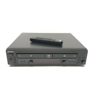
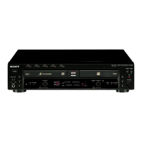
RCD-W10
• IC501 HD64F3064BFBL25 µCOM (CDR Board)
Pin No.
1
2
3 to 5
6
7
8
9
10
11
12
13
14
15
16
17
18
19, 20
21
22
23
24
25
26
27 to 34
35
36 to 43
44
45 to 56
57
58
59
60
61
62
63
64
65
66
67
68
69
70
71
72
73
74
75
76
77
78
I/O
—
O
—
O
I
O
O
I
—
O
O
I
I
O
I
O
—
O
—
O
O
O
O
I/O
—
O
—
O
—
—
O
O
I
I
I
I
—
I
I
—
O
O
O
O
I
I
I
—
—
I
Pin Name
VCL
XCSCDR
NU
XRSTRFP
XREQI
XRDYO
XRSTCDR
FWE
VSS
SDATAO
SDATAO(HOST)
SDATAI(PROM)
SDATAI(HOST)
SCLKO
SUB_SYNC
RSBETA
NU
MIRR/XRC
VSS
AGCON
XRW/R
VRDSW
VWDSW
D8 to D15
VCC
A0 to A7
VSS
A8 to A19
VSS
NU
CS
XLAT
ATIPSYNC
XSTBY
XREST
XP.DOWN
VSS
EXTAL
XTAL
VCC
XAS
XRD
XHWR
XLWR
MD0(H)
MD1(L)
MD2
AVCC
AVREF
KEY
Description
Capacitor connection terminal for the internal power supply
Chip select signal output to the IC201
Not used (fixed at “H”)
Register reset signal output to the IC101
Data request signal from the IC1
Data ready signal to the IC1
Reset signal to the IC201
Flash memory write enable signal input
Ground terminal
Serial data output to the IC101 and IC502
Serial data output to the IC1
Serial data input from the IC502
Serial data input from the IC1
Clock output to the IC101 and IC502
Sub-code sync signal input from the IC201
β measurement circuit reset signal output
Not used (fixed at “H”)
MIRR or RC selection signal output
Ground terminal
AGC enable signal output to the IC101
CD-RW selection signal output to the IC101
Read laser driver time constant selection switch control signal output to the IC101
Write laser driver time constant selection switch control signal output to the IC101
Data bus with the IC201
Power supply (+5V)
Command register selection address signal output to the IC201
Ground terminal
Not used (fixed at “H”)
Ground terminal
Not used
Chip select signal output to the IC502
Data latch signal output to the IC101
ATIP SYNC signal input from the IC201
Not used (fixed at “H”)
System reset signal input
Not used
Ground terminal
Ceramic resonator connection terminal
Ceramic resonator connection terminal
Power supply (+5V)
Not used
Data read signal output to the IC201
Data write signal output to the IC201
Not used
Mode selector (fixed at “H”)
Mode selector (fixed at “L”)
Mode selector (normally fixed at “H”)
Power supply (+5V) for the A/D converter
Reference voltage for the A/D converter
Key scan signal input
 Loading...