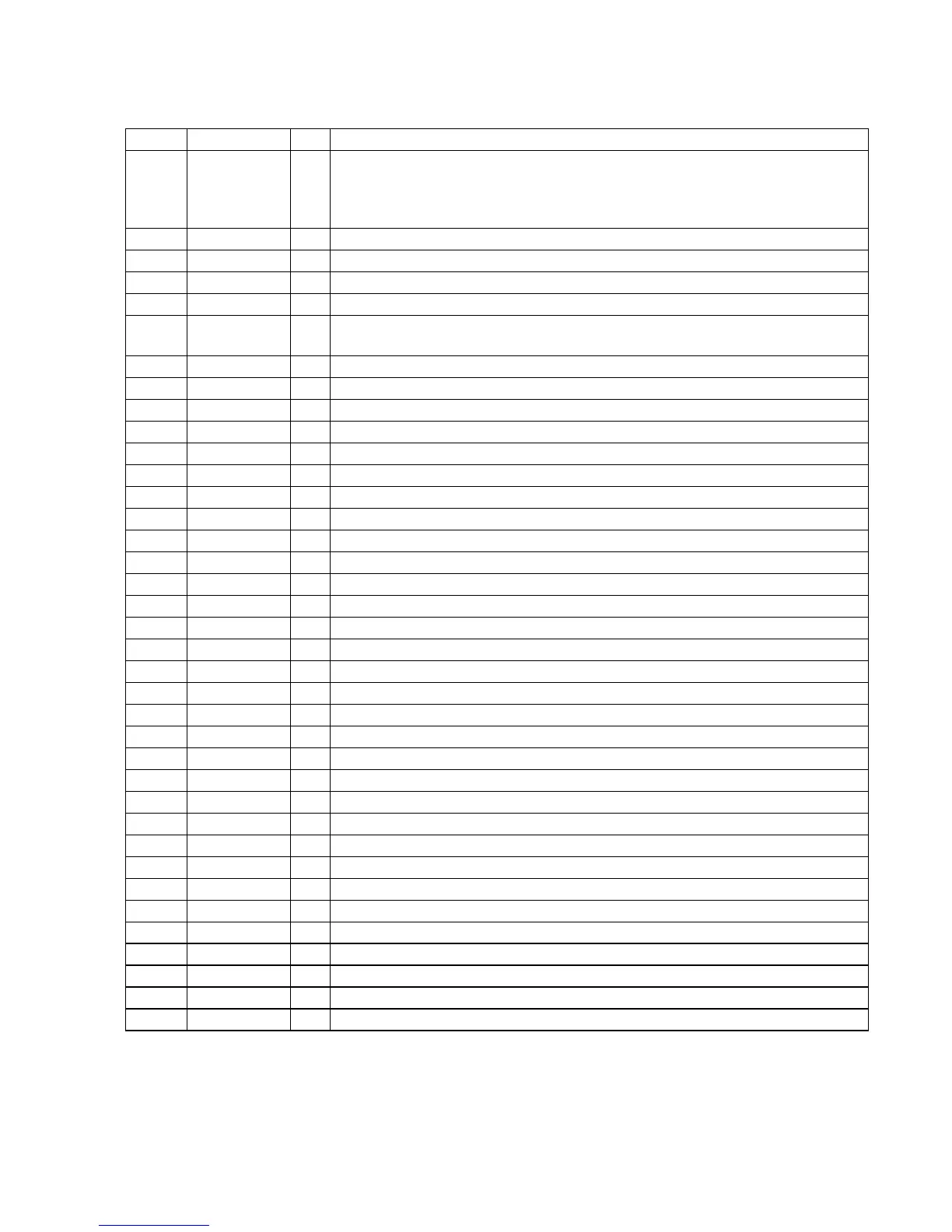
163
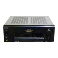
STR-DA5300ES
Pin No.
Pin Name I/O Description
83 to 90
MD12, MD4,
MD11, MD3,
MD10, MD2,
MD9, MD1
I/O Two-way data bus with the flash memory
91
VSS - Ground terminal
92
VDD - Power supply terminal (+3.3V)
93, 94
MD8, MD0 I/O Two-way data bus with the flash memory
95
RAHZ_N - Not used
96 to 98
XTEST2 to
XTEST0
- Not used
99
VSIN_N I Vertical sync signal input terminal Not used
100
HSIN_N I Horizontal sync signal input terminal Not used
101
NC - Not used
102
AVDD - Power supply terminal (+3.3V)
103
ROAnalog video signal (R) output terminal Not used
104
GOAnalog video signal (G) output terminal Not used
105
BOAnalog video signal (B) output terminal Not used
106
IREF - Not used
107
AVSS - Ground terminal
108
NC - Not used
109
VDD - Power supply terminal (+3.3V)
110
VSS - Ground terminal
111 to 116
DR0 to DR5 O Digital video signal (R) output to the video processor
117
VSS - Ground terminal
118
VDD - Power supply terminal (+3.3V)
119 to 124
DG0 to DG5 O Digital video signal (G) output to the video processor
125
VSS - Ground terminal
126
VDD - Power supply terminal (+3.3V)
127to 132
DB0 to DB5 O Digital video signal (B) output to the video processor
133
VSS - Ground terminal
134
FSC - Not used
135
YS_N - Not used
136
VSYNC_N O Vertical sync signal output to the video processor
137
HSYNC_N O Horizontal sync signal output to the video processor
138
BLANK_N O Blanking period signal output to the video processor
139
DOTCLK O Dot clock signal output to the video processor
140
VDD - Power supply terminal (+3.3V)
141
XIN I System clock input terminal (33.2 MHz)
142
XOUT O System clock output terminal (33.2 MHz)
143
VSS - Ground terminal
144
NC - Not used