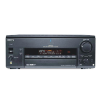
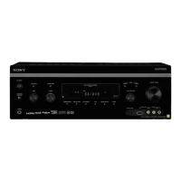
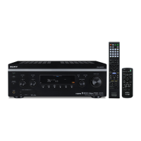
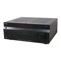
STR-DA6400ES
STR-DA6400ES
4343
For Schematic Diagrams.
Note:
• All capacitors are in μF unless otherwise noted. (p: pF) 50
WV or less are not indicated except for electrolytics and
tantalums.
• All resistors are in Ω and 1/4 W or less unless otherwise
specifi ed.
•
f
: internal component.
• 2 : nonfl ammable resistor.
• C : panel designation.
THIS NOTE IS COMMON FOR PRINTED WIRING BOARDS AND SCHEMATIC DIAGRAMS.
(In addition to this, the necessary note is printed in each block.)
• A : B+ Line.
• B : B– Line.
• H : adjustment for repair.
• Voltages and waveforms are dc with respect to ground
under no-signal (detuned) conditions.
– A-VIDEO board –
no mark : VIDEO 1 mode
– Other boards –
no mark : TUNER
• Voltages are taken with VOM (Input impedance 10 MΩ).
Voltage variations may be noted due to normal production
tolerances.
• Waveforms are taken with a oscilloscope.
Voltage variations may be noted due to normal production
tolerances.
• Circled numbers refer to waveforms.
• Signal path.
F : AUDIO (ANALOG)
J : AUDIO (DIGITAL)
E : VIDEO
For Printed Wiring Boards.
Note:
• X : Parts extracted from the component side.
• Y : Parts extracted from the conductor side.
•
f
: internal component.
• : Pattern from the side which enables seeing.
(The other layers' patterns are not indicated.)
• Indication of transistor.
C
B
These are omitted.
E
Q
B
These are omitted.
CE
Q
Caution:
Pattern face side:
(SIDE B)
Parts face side:
(SIDE A)
Parts on the pattern face side seen from
the pattern face are indicated.
Parts on the parts face side seen from
the parts face are indicated.
• Lead layouts
surface
CSP (Chip Size Package) Lead layout of conventional IC
Caution:
Pattern face side:
(Conductor Side)
Parts face side:
(Component Side)
Parts on the pattern face side seen from
the pattern face are indicated.
Parts on the parts face side seen from
the parts face are indicated.
• D VIDEO, DSP, F-HDMI and NETWORK boards are
multi-layer printed board. However, the patterns of inter-
mediate-layers have not been included in this diagrams.
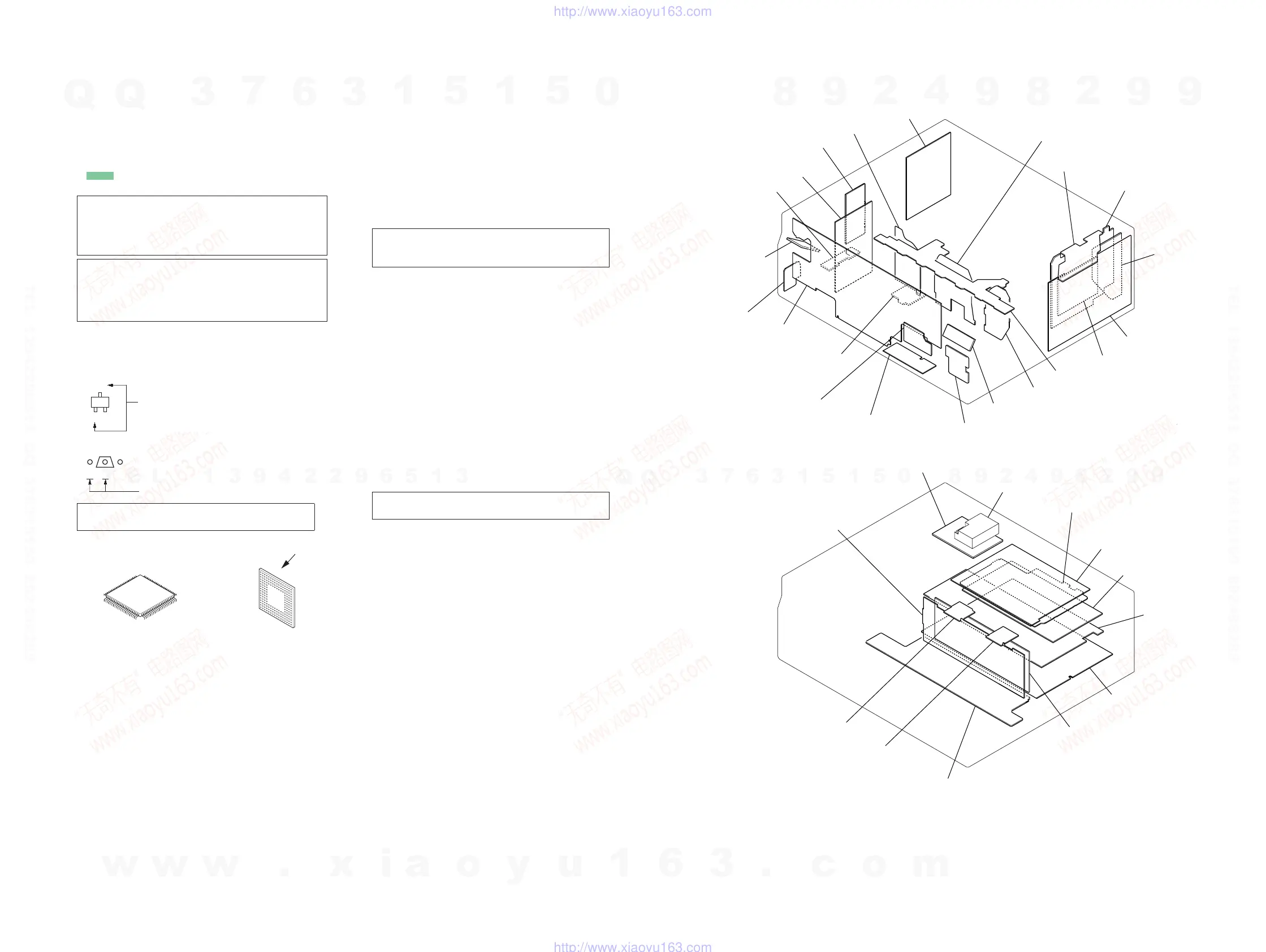
• Circuit Boards Location
∗ Replacement of IC3601 on the D VIDEO board used
in this set requires a special tool.
• The voltage and waveform of CSP (chip size package)
cannot be measured, because its lead layout is different
from that of conventional IC.
∗ Replacement of IC3601 on the D VIDEO board used
in this set requires a special tool.
SPTM board
TUNER (FM/AM)
PROTECTOR (SURR) board
KEY1 board
PROTECTOR (SB) board
AC board
A-VIDEO board
ANALOG board
D VIDEO board
NETWORK board
MAIN board
E-VOL board
CONNECTOR2 board
A-CLASS AMP board
POWER AMP board
CONNECTOR1 board
D CONNECT board
CONTROL board
PROTECTOR (F-C) board
TEMPERATURE
DETECTION board
F-HDMI board
VIDEO2 board
MAIN VOL board
DISPLAY board
DSP board
BIAS board
CIS board
DIGITAL board
ACSW board
HP board
FILTER board
DCDC1 board
DCDC2 board
Note: The components identifi ed by mark 0 or dotted
line with mark 0 are critical for safety.
Replace only with part number specifi ed.
w
w
w
.
x
i
a
o
y
u
1
6
3
.
c
o
m
Q
Q
3
7
6
3
1
5
1
5
0
9
9
2
8
9
4
2
9
8
T
E
L
1
3
9
4
2
2
9
6
5
1
3
9
9
2
8
9
4
2
9
8
0
5
1
5
1
3
6
7
3
Q
Q
TEL 13942296513 QQ 376315150 892498299
TEL 13942296513 QQ 376315150 892498299
http://www.xiaoyu163.com
http://www.xiaoyu163.com