Advanced-control timers (TIM1/TIM8/TIM20) RM0440
1198/2126 RM0440 Rev 4
28.6.11 TIMx capture/compare enable register
(TIMx_CCER)(x = 1, 8, 20)
Address offset: 0x020
Reset value: 0x0000 0000
Bit 3 OC3PE: Output compare 3 preload enable
Bit 2 OC3FE: Output compare 3 fast enable
Bits 1:0 CC3S[1:0]: Capture/compare 3 selection
This bit-field defines the direction of the channel (input/output) as well as the used input.
00: CC3 channel is configured as output
01: CC3 channel is configured as input, tim_ic3 is mapped on tim_ti3
10: CC3 channel is configured as input, tim_ic3 is mapped on tim_ti4
11: CC3 channel is configured as input, tim_ic3 is mapped on tim_trc. This mode is working
only if an internal trigger input is selected through TS bit (TIMx_SMCR register)
Note: CC3S bits are writable only when the channel is OFF (CC3E = ‘0’ in TIMx_CCER).
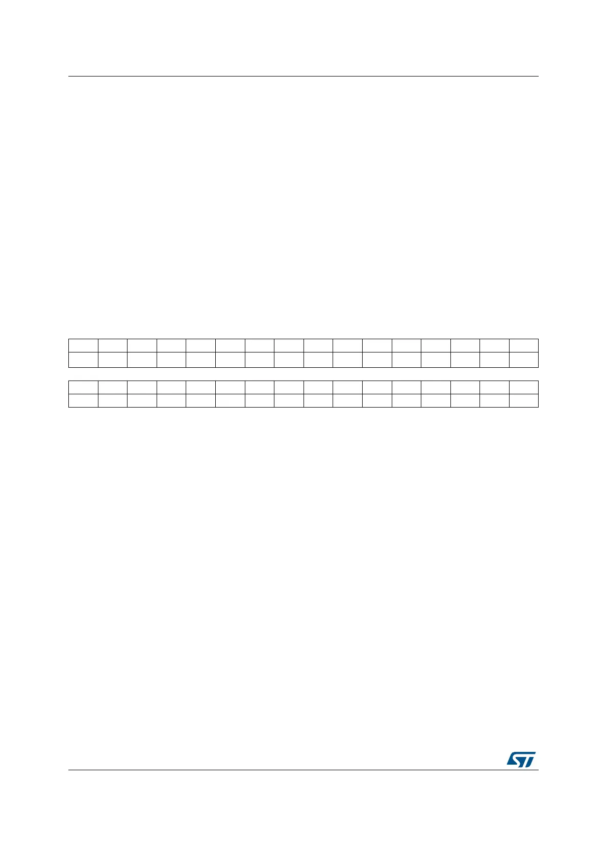
31 30 29 28 27 26 25 24 23 22 21 20 19 18 17 16
Res. Res. Res. Res. Res. Res. Res. Res. Res. Res. CC6P CC6E Res. Res. CC5P CC5E
rw rw rw rw
1514131211109876543210
CC4NP CC4NE CC4P CC4E CC3NP CC3NE CC3P CC3E CC2NP CC2NE CC2P CC2E CC1NP CC1NE CC1P CC1E
rw rw rw rw rw rw rw rw rw rw rw rw rw rw rw rw
Bits 31:22 Reserved, must be kept at reset value.
Bit 21 CC6P: Capture/compare 6 output polarity
Refer to CC1P description
Bit 20 CC6E: Capture/compare 6 output enable
Refer to CC1E description
Bits 19:18 Reserved, must be kept at reset value.
Bit 17 CC5P: Capture/compare 5 output polarity
Refer to CC1P description
Bit 16 CC5E: Capture/compare 5 output enable
Refer to CC1E description
Bit 15 CC4NP: Capture/compare 4 complementary output polarity
Refer to CC1NP description
Bit 14 CC4NE: Capture/compare 4 complementary output enable
Refer to CC1NE description
Bit 13 CC4P: Capture/compare 4 output polarity
Refer to CC1P description
Bit 12 CC4E: Capture/compare 4 output enable
Refer to CC1E description
Bit 11 CC3NP: Capture/compare 3 complementary output polarity
Refer to CC1NP description

 Loading...