Reset and clock control (RCC) RM0440
312/2126 RM0440 Rev 4
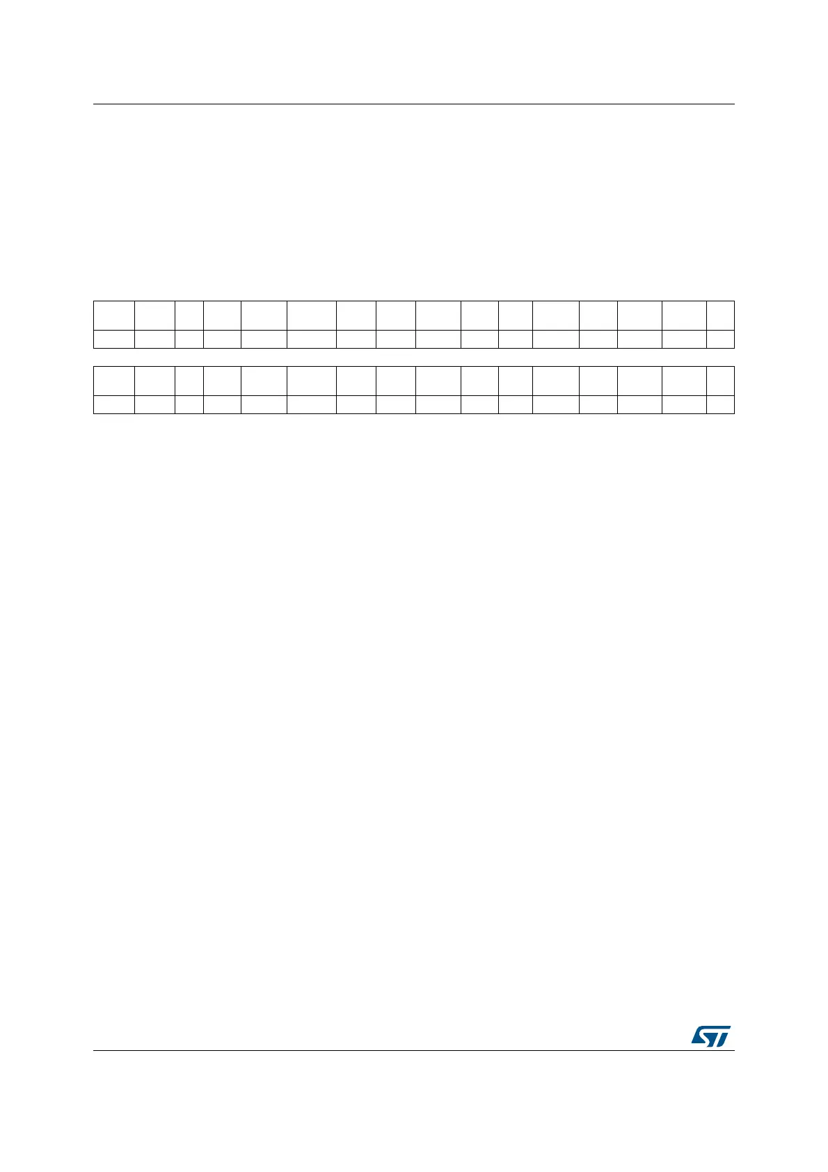
7.4.17 APB1 peripheral clock enable register 1 (RCC_APB1ENR1)
Address: 0x58
Reset value: 0x0000 0400
Access: no wait state, word, half-word and byte access
Note: When the peripheral clock is not active, the peripheral registers read or write access is not
supported.
31 30 29 28 27 26 25 24 23 22 21 20 19 18 17 16
LPTIM1
EN
I2C3
EN
Res.
PWR
EN
Res. Res.
FDCAN
EN
Res.
USB
EN
I2C2
EN
I2C1
EN
UART5
EN
UART4
EN
USART3
EN
USART2
EN
Res.
rw rw rw rw rw rw rw rw rw rw rw
15 14 13 12 11 10 9 8 7 6 5 4 3 2 1 0
SPI3
EN
SPI2
EN
Res. Res.
WWDG
EN
RTCAPB
EN
Res.
CRS
EN
Res. Res.
TIM7
EN
TIM6
EN
TIM5
EN
TIM4
EN
TIM3
EN
TIM2
EN
rw rw rs rw rw rw rw rw rw rw rw
Bit 31 LPTIM1EN: Low power timer 1 clock enable
Set and cleared by software.
0: LPTIM1 clock disabled
1: LPTIM1 clock enabled
Bit 30 I2C3EN: I2C3 clock enable
Set and cleared by software.
0: I2C3 clock disabled
1: I2C3 clock enabled
Bit 29 Reserved, must be kept at reset value.
Bit 28 PWREN: Power interface clock enable
Set and cleared by software.
0: Power interface clock disabled
1: Power interface clock enabled
Bits 27:26 Reserved, must be kept at reset value.
Bit 25 FDCANEN: FDCAN clock enable
Set and cleared by software.
0: FDCAN clock disabled
1: FDCAN clock enabled
Bit 24 Reserved, must be kept at reset value.
Bit 23 USBEN: USB device clock enable
Set and cleared by software.
0: USB device clock disabled
1: USB device clock enabled
Bit 22 I2C2EN: I2C2 clock enable
Set and cleared by software.
0: I2C2 clock disabled
1: I2C2 clock enabled

 Loading...


