RM0440 Rev 4 363/2126
RM0440 General-purpose I/Os (GPIO)
368
Reset value: 0x0000 0000
9.4.8 GPIO port configuration lock register (GPIOx_LCKR)
(x = A to G)
This register is used to lock the configuration of the port bits when a correct write sequence
is applied to bit 16 (LCKK). The value of bits [15:0] is used to lock the configuration of the
GPIO. During the write sequence, the value of LCKR[15:0] must not change. When the
LOCK sequence has been applied on a port bit, the value of this port bit can no longer be
modified until the next MCU reset or peripheral reset.
Note: A specific write sequence is used to write to the GPIOx_LCKR register. Only word access
(32-bit long) is allowed during this locking sequence.
Each lock bit freezes a specific configuration register (control and alternate function
registers).
Address offset: 0x1C
Reset value: 0x0000 0000
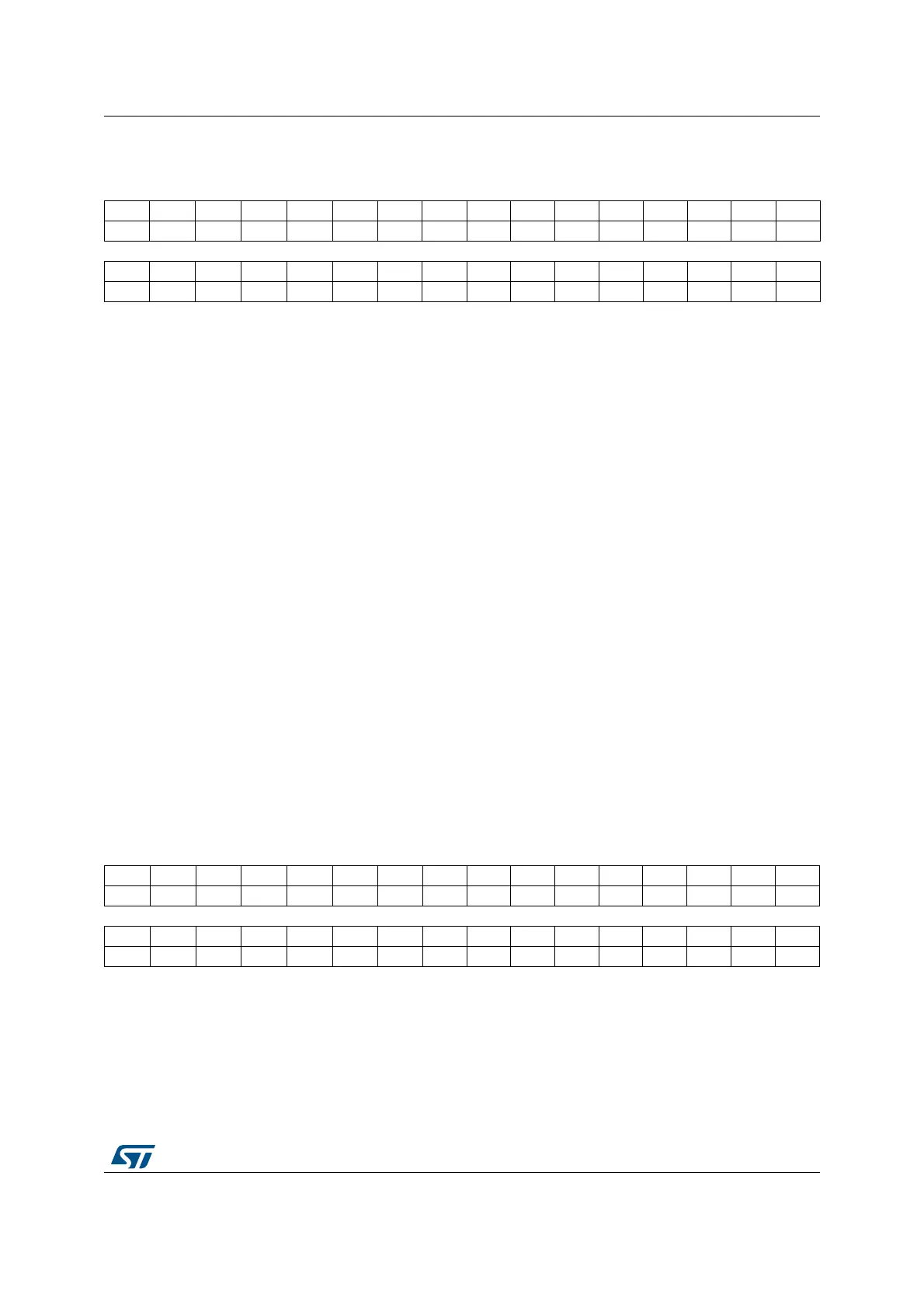
31 30 29 28 27 26 25 24 23 22 21 20 19 18 17 16
BR15 BR14 BR13 BR12 BR11 BR10 BR9 BR8 BR7 BR6 BR5 BR4 BR3 BR2 BR1 BR0
wwwwwwwwwwwwwwww
1514131211109876543210
BS15 BS14 BS13 BS12 BS11 BS10 BS9 BS8 BS7 BS6 BS5 BS4 BS3 BS2 BS1 BS0
wwwwwwwwwwwwwwww
Bits 31:16 BR[15:0]: Port x reset I/O pin y (y = 15 to 0)
These bits are write-only. A read to these bits returns the value 0x0000.
0: No action on the corresponding ODx bit
1: Resets the corresponding ODx bit
Note: If both BSx and BRx are set, BSx has priority.
Bits 15:0 BS[15:0]: Port x set I/O pin y (y = 15 to 0)
These bits are write-only. A read to these bits returns the value 0x0000.
0: No action on the corresponding ODx bit
1: Sets the corresponding ODx bit
31 30 29 28 27 26 25 24 23 22 21 20 19 18 17 16
Res. Res. Res. Res. Res. Res. Res. Res. Res. Res. Res. Res. Res. Res. Res. LCKK
rw
15 14 13 12 11 10 9 8 7 6 5 4 3 2 1 0
LCK15 LCK14 LCK13 LCK12 LCK11 LCK10 LCK9 LCK8 LCK7 LCK6 LCK5 LCK4 LCK3 LCK2 LCK1 LCK0
rw rw rw rw rw rw rw rw rw rw rw rw rw rw rw rw

 Loading...


