configuration should only be updated when the
s state. The RX state will be active
when the chip is in receive mode. Likewise, TX
is active when the chip is transmitting.
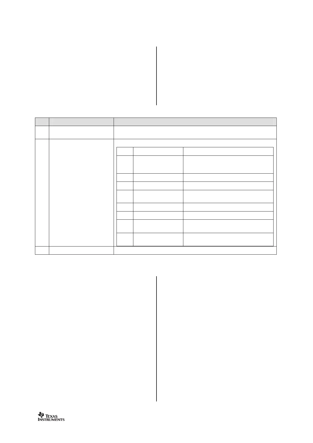
The last four bits (3:0) in the status b
bit in the header byte is
contains the number of bytes available for
reading from the RX FIFO. For write
bit in the header byte is
contains the number of bytes that can be
written to the TX FIFO. When
bytes are available/free.
gives a status byte summary.
Stays high until power and crystal have stabilized. Should always be low when using
Indicates the current main stat
(Also reported for some transitional states
instead of SETTLING or CALIBRATE)
Frequency synthesizer is on, ready to start
Frequency synthesizer calibration is running
RX FIFO has overflowed. Read out any
useful data, then flush the FIFO with
TX FIFO has underflowed. Acknowledge with
FIFO_BYTES_AVAILABLE[3:0]
The number of bytes available in the RX FIFO or free bytes in the TX FIFO
The configuration registers of the
located on SPI addresses from 0x
It is highly recommended to use
The detailed description of
each register is found in Section
. All configuration registers can be
both written to and read. The
if the register should be written to or read.
When writing to registers, the status byte is
pin each time a header byte or
data byte is transmitted on the
reading from registers, the status byte is sent
Registers with consecutive addresses can be
accessed in an efficient way by setting the
internal address counter. This
incremented by one each new byte (every 8
clock pulses). The burst access is either a
read or a write access and must be terminated
For register addresses in the range 0x30
0x3D, the burst bit is used to select between
tus registers, burst bit is one, and command
strobes, burst bit is zero (see
). Because of this, burst access is not
When reading register fields
interface while the register fields are