A crystal in the frequency range 26
must be connected between the
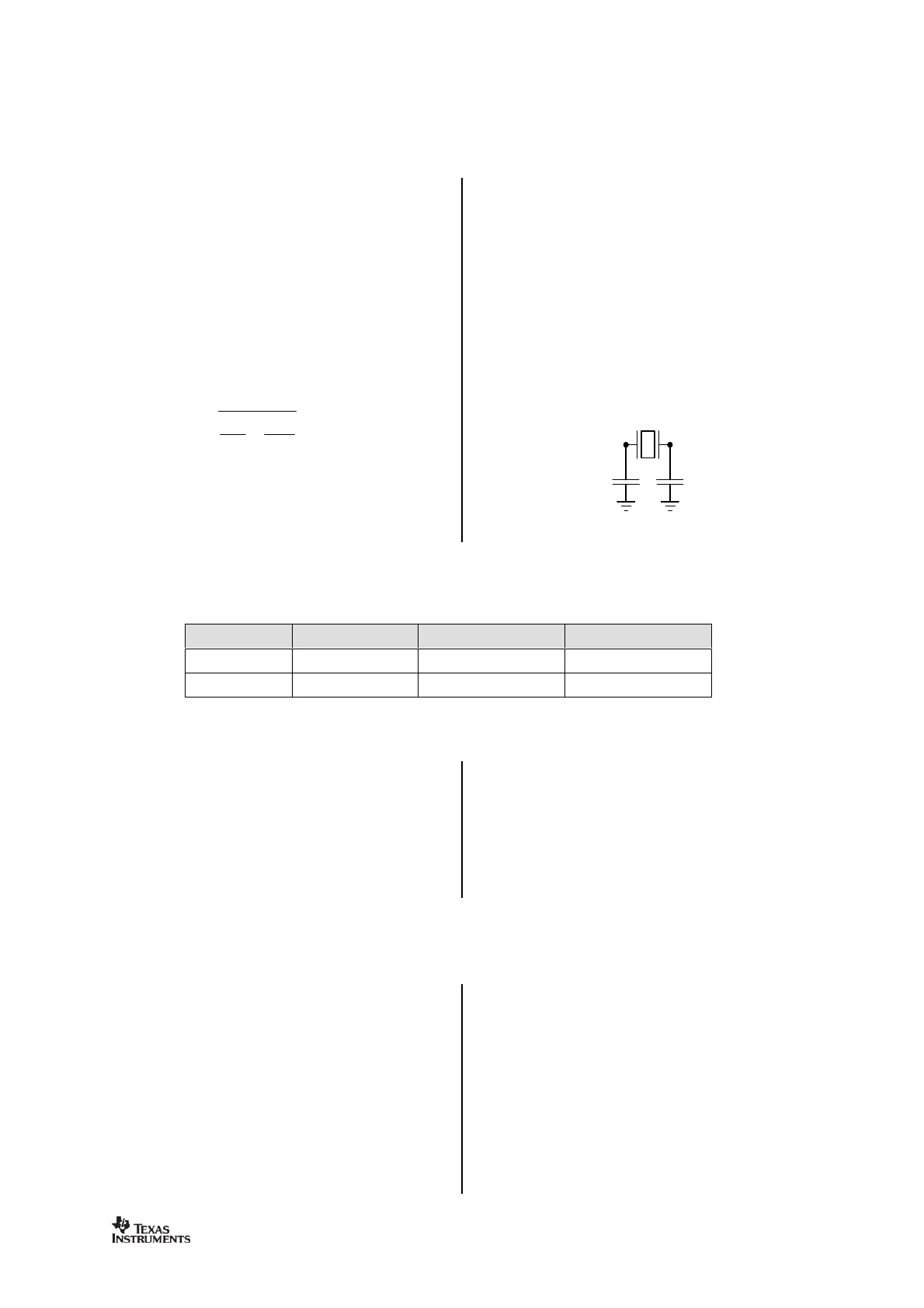
pins. The oscillator is des
parallel mode operation of the crystal. In
addition, loading capacitors (C81 and C101)
for the crystal are required. The loading
capacitor values depend on the total load
, specified for the crystal. The
total load capacitance seen
crystal terminals should equal C
crystal to oscillate at the specified frequency.
The parasitic capacitance is constituted by pin
input capacitance and PCB stray capacitance.
Total parasitic capacitance is typi
The crystal oscillator circuit is shown in
. Typical component values for different
The crystal oscillator is am
This means that a high current is used to start
up the oscillations. When the amplitude builds
up, the current is reduced to what is necessary
to maintain approximately 0.4
swing. This ensures a fast start
ive level to a minimum. The ESR of the
crystal should be within the specification in
order to ensure a reliable start
ernatively be operated with a
reference signal from 26 to 27 MHz instead of
a crystal. This input clock can either be a full
swing digital signal (0 V to VDD) or a sine
The reference signal must be connected to the
input. The sine wave must be
signal this capacitor can be omitted.
and C101 can be omitted when using a
The balanced RF input and output of
share two common pins and are designed for
cost matching and balun network
on the printed circuit board. The receive
transmit switching at the
eliminating the need for an external RX/TX
A few passive external components combined
with the internal RX/TX switch/termination
circuitry ensures match in both RX and TX
nput/output, the chip can be connected to a
ended antenna with few external low
cost capacitors and inductors.
The passive matching/filtering network
should have the following
differential impedance as seen from the RF