configuration data based on selected system
parameters are most easily found by using the
descriptions of the registers are given in the
following tables. After chip reset, all the
registers have default values as shown in the
The optimum register setting might
differ from the default value. Af
registers that shall be different from the default
value therefore needs to be programmed
through the SPI interface.
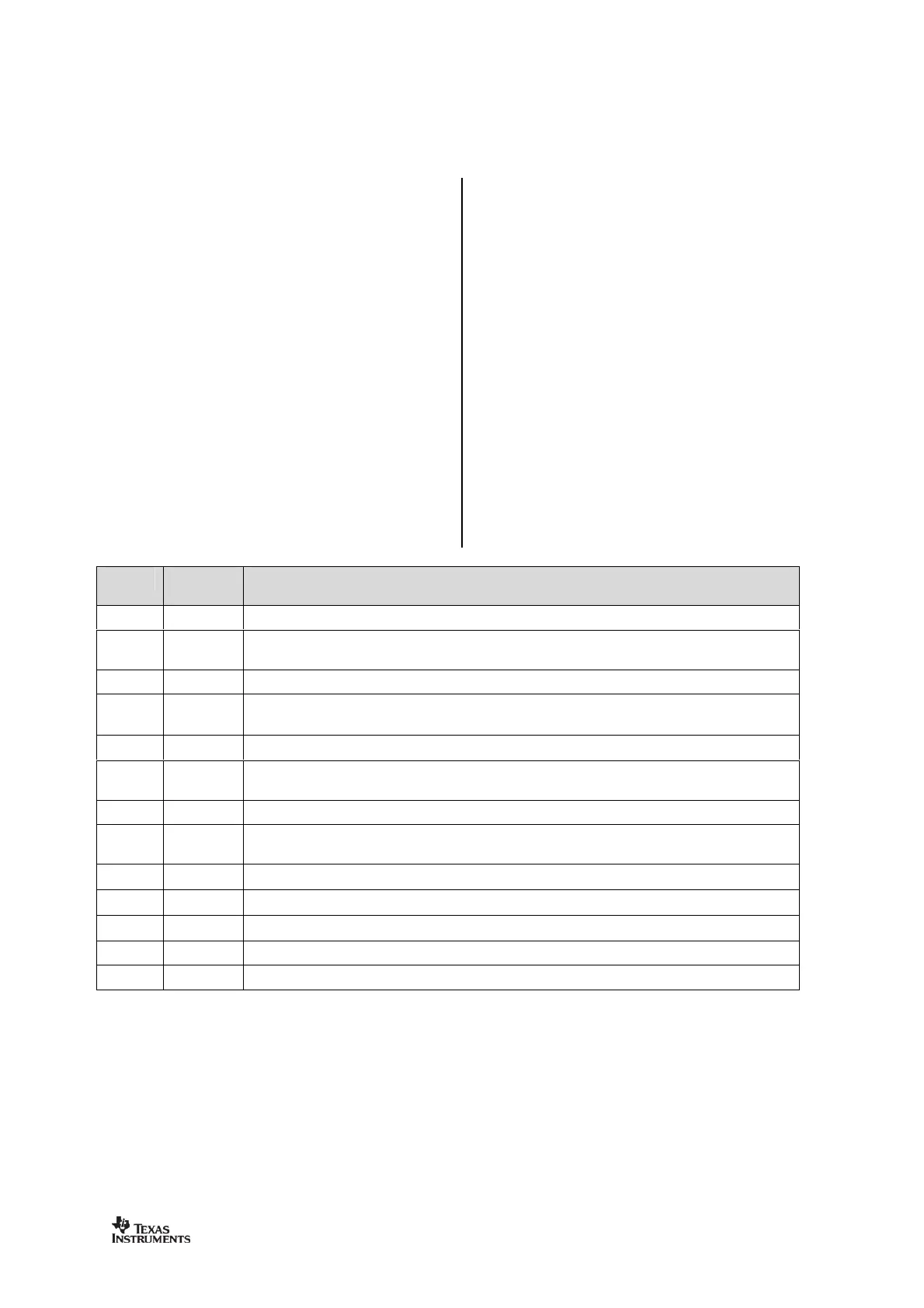
There are 13 command strobe r
initiate the change of an internal state or
ode. There are 47 normal 8
registers are for test purposes only, and need
tatus registers, which are
. These registers, which are
only, contain information about the status
The two FIFOs are accessed through one
register. Write operations write to the TX FIFO,
while read operations read from the RX FIFO.
to a register or the TX FIFO, a
summarizes the SPI address space.
The address to use is given by adding the
base address to the left and the b
bits on the top. Note that the burst bit has
different meaning for base addresses above
Enable and calibrate frequency synthesizer (if
=1). If in RX (with CCA):
Go to a wait state where only the synthesizer is running (for quick RX / TX turnaround).
Turn off crystal oscillator.
Calibrate frequency synthesizer and turn it off
can be strobed from IDLE mode without
setting manual calibration mode (
Enable RX. Perform calibration first if coming from IDLE and
IDLE state: Enable TX. Perform calibration first if
If in RX state and CCA is enabled: Only go to TX if channel is clear.
Exit RX / TX, turn off frequency synthesizer and exit Wake
Start automatic RX polling sequence (Wake
Radio) as described in Section
Enter power down mode when
Flush the RX FIFO buffer. Only issue
Flush the TX FIFO buffer. Only issue
in IDLE or TXFIFO_UNDERFLOW states.
No operation. May be used to get access to the chip status byte.