EasyManuals Logo

Texas Instruments CC2500 User Manual

Texas Instruments CC2500
96 pages
To Next Page IconTo Next Page
To Previous Page IconTo Previous Page
Page #25 background imageLoading...
Page #25 background image
CC2500
S
WRS040
C
Page
25
of
89
When using OOK
modulation the first two
entries into this table are used (index 0
and index 1).
Since the
PATABLE
is an 8
-
byte table, the
table is written and read from the lowest
setting (0) to the highest (7), one byte at a
time. An index counter is used to control th
e
access to the table. This counter is
incremented each time a byte is read or
written to the table, and set to the lowest index
when
CSn
is high. When the highest value is
reached the counter restarts at 0.
The access to the
PATABLE
is either single
byte
or burst access depending on the burst
bit. When using burst access the index counter
will count up; when reaching 7 the counter will
restart at 0. The
R
/
W
bit controls whether the
access is a write access (
R/W
=0) or a read
access (
R/W
=1).
If one byte is
written to the
PATABLE
and this
value is to be read out then
CSn
must be set
high before the read access in order to set the
index counter back to zero.
Note that the content of the
PATABLE
is lost
when entering the SLEEP state, except for the
first byte
(index 0).
See Section
24
on page
46
for output power
programming details.
Figure
9
: Register Access Types
11
Microcontroll
er Interface and Pin Configuration
In a typical system,
CC2500
will interface to a
microcontroller. This microcontroller must be
able to:
Program
CC2500
into different modes
Read and write buffered data
Read back status information via the 4
-
wire
SPI
-
b
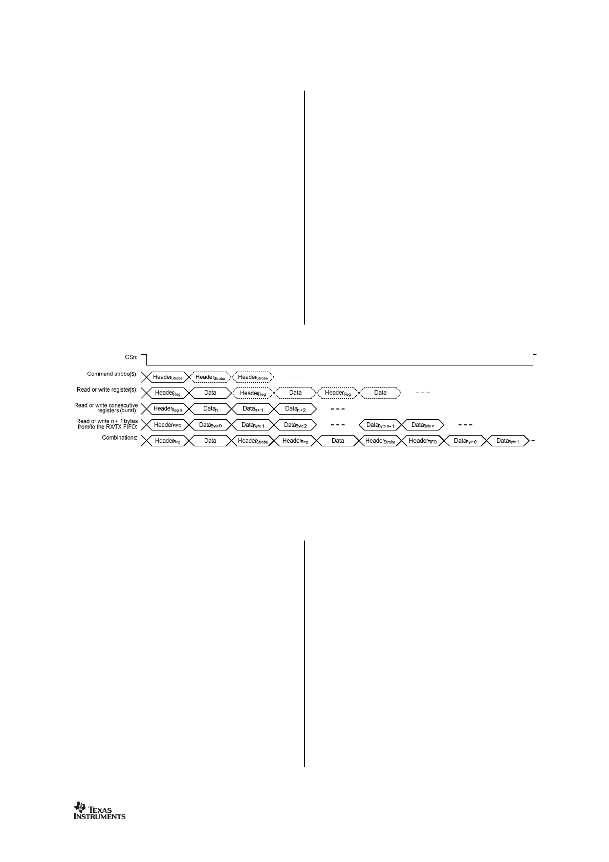
us configuration interface (
SI
,
SO
,
SCLK
and
CSn
)
11.1
Configuration Interface
The microcontroller uses four I/O pins for the
SPI configuration interface (
SI
,
SO
,
SCLK
and
CSn
). The SPI is described in Section
1
0
on
page
21
.
11.2
General Control and Status Pins
The
CC2500
has two dedicated configurable
pins
(
GDO0
and
GDO2
)
and one shared pin
(
GDO1
)
that can output internal status
information useful for control software. These
pins can be use
d to generate interrupts on the
MCU. See Section
28
on page
51
for more
details on the signals that can be programmed.
GDO1
is
shared
with the
SO
pin in the SPI
interface. The default
setting for
GDO1/SO
is 3
-
state output. By selecting any other of the
programming options the
GDO1/SO
pin will
become a generic pin. When
CSn
is low, the
pin will always function as a normal
SO
pin.
In the synchronous and asynchronous serial
modes, the
GDO
0
pin is used as a serial TX
data input pin while in transmit mode.

Table of Contents

Questions and Answers:

Question and Answer IconNeed help?

Do you have a question about the Texas Instruments CC2500 and is the answer not in the manual?

Texas Instruments CC2500 Specifications

General IconGeneral
BrandTexas Instruments
ModelCC2500
CategoryTransceiver
LanguageEnglish

Related product manuals