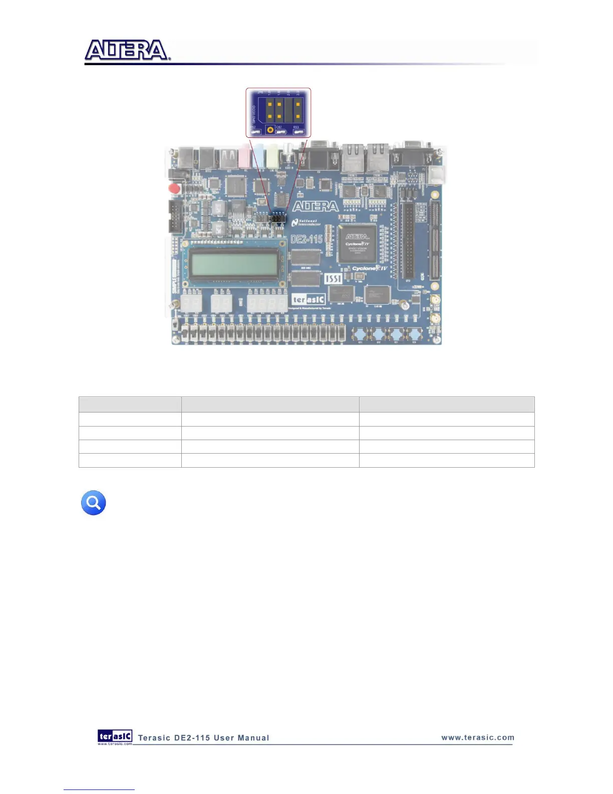
Figure 4-13 HSMC VCCIO supply voltage setting header
Table 4-8 Jumper Settings for different I/O Standards
Note: Users that connect a daughter card on the HSMC connector need to pay close
attention on the I/O standard between DE2-115 HSMC connector pins and daughter card system.
For example, if the I/O standard of HSMC pins on DE2-115 board is set to 1.8V, a daughter card
with 3.3V I/O standard may not work properly on DE2-115 board due to I/O standard mismatch.
Additionally, when LVDS is used as the I/O standard of the HSMC connector, the LVDS receivers
need to assemble a 100 Ohm resistor between two input signals for each pairs as shown in Figure
4-14. Table 4-9 shows all the pin assignments of the HSMC connector.