4
4
.
.
1
1
5
5
T
T
V
V
D
D
e
e
c
c
o
o
d
d
e
e
r
r
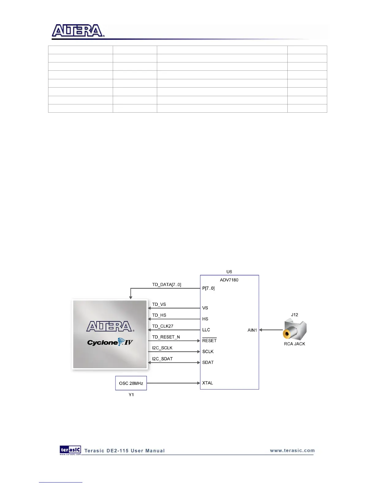
The DE2-115 board is equipped with an Analog Device ADV7180 TV decoder chip. The ADV7180
is an integrated video decoder that automatically detects and converts a standard analog baseband
television signals (NTSC, PAL, and SECAM) into 4:2:2 component video data compatible with the
8-bit ITU-R BT.656 interface standard. The ADV7180 is compatible with a broad range of video
devices, including DVD players, tape-based sources, broadcast sources, and security/surveillance
cameras.
The registers in the TV decoder can be programmed by a serial I2C bus, which is connected to the
Cyclone IV E FPGA as indicated in Figure 4-29. Note that the I2C address W/R of the TV decoder
(U6) is 0x40/0x41. The pin assignments are listed in Table 4-24. Detailed information of the
ADV7180 is available on the manufacturer‟s website, or in the DE2_115_datasheets\TV Decoder
folder on the DE2-115 System CD.
Figure 4-29 Connections between FPGA and TV Decoder