Frequency Hz
Time
ti
Fore-backward dead time
Figure 8-15-1 Schematic diagram of forward and reverse switching
8.16 Dynamic braking
When the motor decelerates, if the load is too large, the deceleration time is too short, etc., the bus voltage
of the inverter may rise to the overvoltage level. At this time, on the premise of connecting the braking resistor,
the overvoltage fault can be avoided by turning on the dynamic braking.
8.17 Frequency detection output (FDT)
It is used to set the detection value of the output frequency and the hysteresis value of the release of the
output action. The hysteresis value is only valid during the deceleration process, and the detection during the
acceleration process does not lag behind.
8.18 Zero current detection
Used to set the zero detection value of the output current.
function
code
name
default value
Predetermined area
Parameter
Description
F8.16
Action voltage of braking
unit
720V (440V series)
360V (230V series)
440V series: (650 ~ 750) V
230V series: (320 ~ 380) V
--
F8.17
Dynamic braking option
0
0 ~ 1
0: no action
1: action
F8.18
Energy consumption
braking utilization rate
80.0%
(0.0~100.0)%
--
function code
name
default value
Predetermined area
Parameter Description
F6. 20
FDT1 level
50.00Hz
0.00Hz ~F0.07
-
F6. 21
FDT1 hysteresis
5.0%
(0.0~100.0)%
100% relative to the maximum
output frequency
F6. 22
FDT2 level
25.00Hz
0.00Hz ~F0.07
-
F6. 23
FDT2 hysteresis
5.0%
(0.0~100.0)%
100% relative to the maximum
output frequency
function code
name
default value
Predetermined area
Parameter Description
F8.20
5.0%
(0.0~300.0)%
--
F8.21
Zero current detection
delay time
0.10s
(0.00 ~ 600.00)s
--
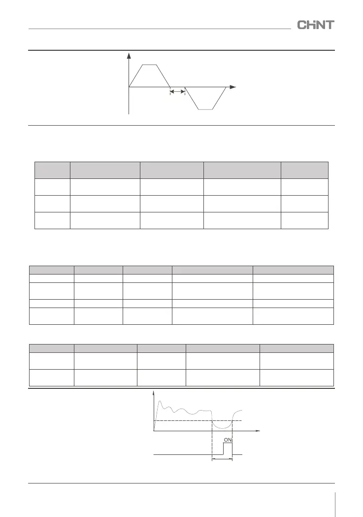
Zero current detection
value
Output current
Zero current
detection value
Zero current
detection signal
Zero current
detection delay time
Time
Figure 8-18-1 Schematic diagram of zero current detection
063
NVF2G-S Series Inverter User's Guide
 Loading...