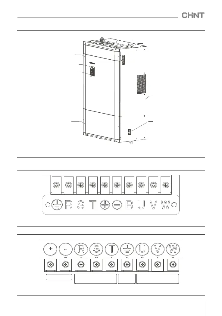
Panel (Top)
Panel base
Keyboard
Panel(Bottom)
INSTALL HOLE
RINGS
SHELL
NAMEPLATE
Figure 4.5 NVF2G-S-315/TS4 ~NVF2G-S400/TS4 external parts diagram
4.2 Main circuit terminal description
(1) Three-phase (380 ~ 440 ) V series (NVF2G-S -1.5/PS4 ~ 30/PS4 )
Figure 4.6 Main circuit terminal NVF2G-S-1.5/PS4 ~ 30/PS4
(2) Three-phase (380 ~ 440 ) V series (NVF2G-S -30/TS4 ~ 45/PS4 )
DC BUS
3PHASE INPUT
3PHASE OUTPUT
GROUND
Figure 4.7 Main circuit terminals NVF2G-S-30/TS4 ~ 45/PS4
009
NVF2G-S Series Inverter User's Guide
 Loading...