EasyManua.ls Logo

Denon LA-3500 - Page 49

Denon LA-3500
92 pages
Print Icon
To Next Page IconTo Next Page
To Previous Page IconTo Previous Page
Loading...
-------------------------------------------LA-3500
-
IC
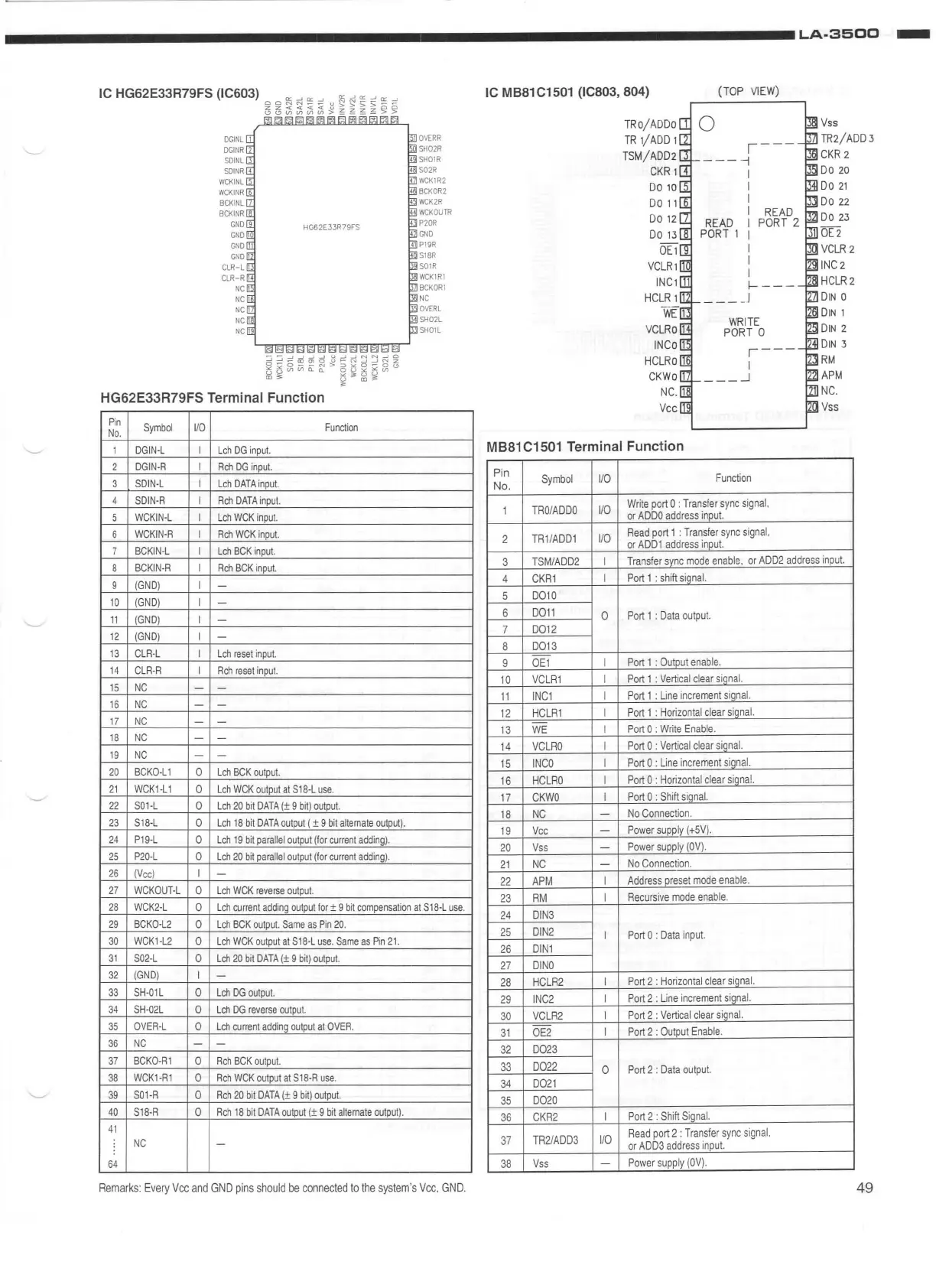
HG62E33R79FS (IC603)
"'
__,
"'
__,
g:;
,-:
9::
""
9::
""
~
~~
~<<t:~~~~§?~
l!l~VlVJVlVl>---
~
W
CKI
NL
BCKINL
HG62E3
3
R79FS
HG62E33R79FS Terminal Function
Pin
Symbol
uo
Function
No
.
1
DGIN-L
I
Leh
DG
input.
2
DGIN-R
I
Reh
DG
input.
3
S
DI
N-L
I L
eh
DATA
input.
4
SD
I
N-R
I
Reh
DATA
input.
5
WCKIN-L
I
L
eh
WCK
input.
6
WCK
I
N-R
I
Reh
WCK
input.
7
BCKIN-L
I L
eh
BCK
input.
8
BCKIN-R
I
Reh
BCK
input.
9
(GN
D)
I -
10
(GND)
I -
11
(GND)
I
-
12
(GND)
I
-
13
CLR-
L
I L
eh
reset
input.
14
CLR-R
I
Reh
reset
input.
15
NC
-
16
NC
-
-
17
NC
18
NC
19
NC
-
20
BCKO-L1
0
Leh
BCK
output.
21
WCK1-
L1
0
L
eh
WCK
output
at
S18-L
use.
22
SOH 0
Leh
20
bit
DATA
(+
9
bit)
output.
23
St8
-L
0
L
eh
18
bit
DATA
output
( + 9
bit
alternate
output).
24
P19-L
0
Leh
19
bit
parallel
output
(for
current
adding)
.
25
P20
-L
0
Leh
20
bit
parallel
output
(fo
r
current
adding).
26
(Vee)
I
-
27
WCKOUT-L
0
Le
h
WCK
reverse
output.
4
BCKOR2
4
WCK2R
'4
WCKOUTR
WCK1R1
BCKOR1
NC
OVERL
SH02L
SH01
L
28
WCK2
-L
0
Le
h
current
adding
output
for± 9
bit
compensation
at
S18
-L
use.
29
BCKO
-
L2
0
Leh
BCK
output.
Same
as
Pin
20.
30
WCK1-L2
0 L
eh
WCK
output
at
S18-L
use.
Same
as
P
in
21.
31
502-L
0
Leh
20
bit
DATA
(+
9
bit)
output.
32
(GN
D)
I
-
33
5H-01L
0
Leh
DG
output.
34
5H-02L
0
Leh
DG
reverse
output.
35
OVER-L
0
Leh
current
adding
output
at
OVER.
36
NC
-
-
37
BCKO
-R
1
0 R
eh
BCK
output.
38
WCK1-R1
0
Reh
WCK
output
at
518-R
use.
39
501-R
0
Reh
20
bit
DATA
(+
9
bit)
output.
40
518
-R
0
Reh
18
bit
DATA
output(+
9
bit
alternate
output).
41
NC
-
64
Remarks:
E
very
Vee
and
GND
pins
should
be
connected
to
the
system
's
Vee.
GND.
IC
M881C1501(IC803,804)
(TOP V
IEW
)
TRo/ADDo
TR
1/ADD
1
TSM
/
ADD2
CKR
1
Do
10
Do
11
Do12
VCL
R1
i----
---
---j
I
I
I
I
READ
READ
I
PORT 2
PORT
1
I
I
I
I
~-
-
-
___
_ J
WRITE
PORT 0
,---
I
___
_J
MB81C1501 Terminal Function
P
in
Symbol
No.
1
/0
Funct
ion
1
TAO
/
ADDO
1
/0
Write
port
O :
Transfer
sync
signal.
or
ADDO
address
i
nput.
2
TR1
/
ADD1
1/0
Read
port
1 :
Transfer
sync
signal.
or
ADD1
address
input.
VC
LR
2
IN
C2
HCLR2
DIN
0
DIN
1
DIN
2
DIN
3
RM
APM
NC.
Vss
3
TSM/ADD2
I
Transfer
sync
mode
enable.
or
ADD2
address
input.
4
CKR1
I
Port
1
:
shift
sianal.
5
D010
6
D011
0
P
ort
1
:
Data
output.
7
D012
8
D013
9
OE1
I
Po
rt
1 :
Output
enable.
10
VC
LR1
I
Port
1 :
Vertical
clear
signal.
11
INC1
I
Port
1 : L
ine
increment
sianal.
12
HCLR1
I
Port
1 :
Hor
i
zon
tal
clear
sianal.
13
WE
I
Port
0 :
Write
E
nable.
14
VCLRO
I
Port
O :
Vertical
clear
sianal.
15
INCO
I
Port
O :
Line
in
cre
ment
sianal.
16
HCLRO
I
Port
O :
Horizontal
clear
siana
l.
17
CKWO
I
Port
0 :
Shift
sianal.
18
NC
No
Connection.
19
Vee
Power
supp
ly
(+SV).
20
Vss
Po
wer
supply
(OV)
.
21
NC
No
Connection
.
22
APM
I
Address
preset
mode
enable.
23
RM
I
Recurs
ive
mode
enable.
24
DIN
3
25
DIN2
I
Port
O :
Data
input.
26
DIN1
27
DINO
28
HCLR2
I
Port
2 :
Horizontal
clear
signal.
29
INC2
I
Port
2 :
Line
incre
men
t
sianal.
30
VCLR2
I
P
ort
2 :
Vertical
clear
s
ignal.
31
OE2
I
Port
2 :
Output
E
nable.
32
D023
33
D022
0
Port
2 :
Da
ta
output.
34
D021
35
D020
36
CKR2
I
Port
2 :
Shift
Signal.
37
TR
2/A
DD3
1/0
Read
port
2 :
Transfer
sync
signal.
or
ADD3
address
input.
38
Vss
Power
supply
(OV).
49

Table of Contents