Technical Manual &
Cabling Instructions
Page 18 / MAN000596
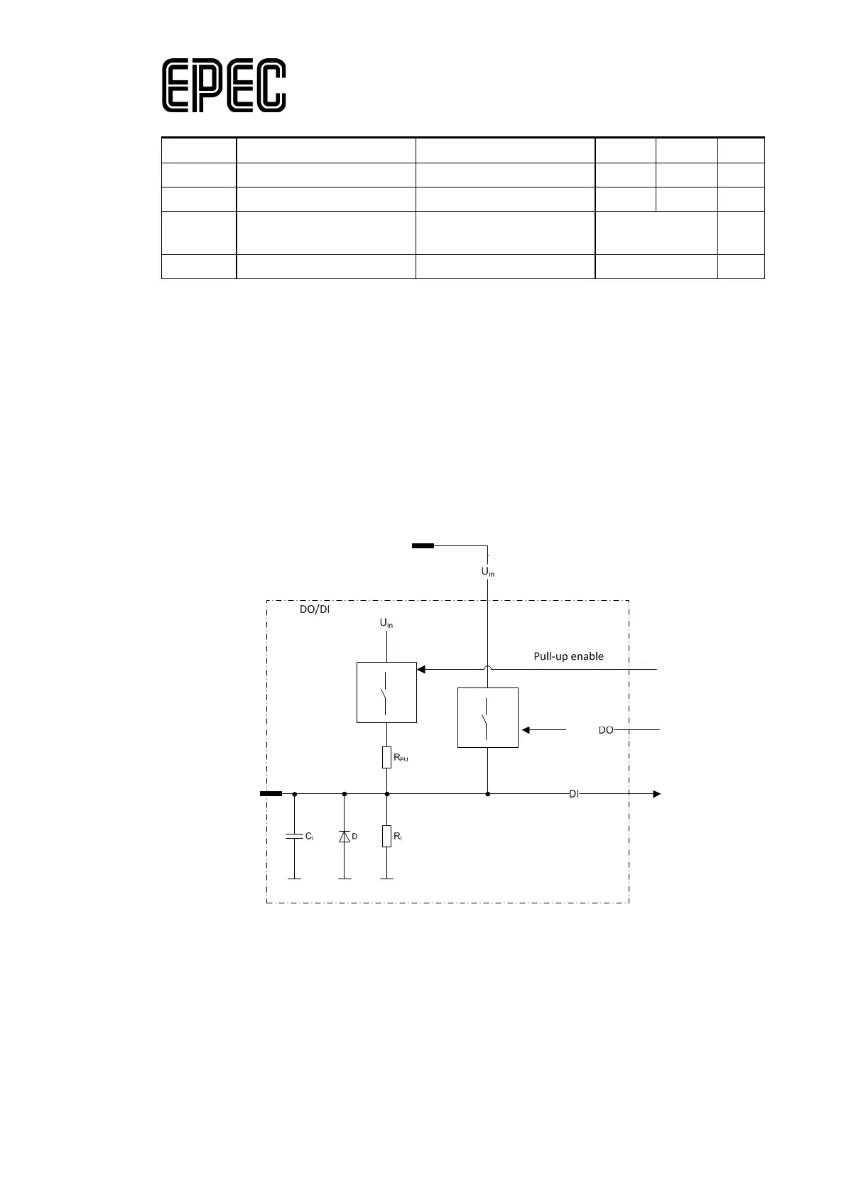
DO/DI
Epec Oy reserves all rights for improvements without prior notice
Epec Oy
Tiedekatu 6
FIN-60320 Seinäjoki
Postal address
PL/P.O.Box 194
FIN-60101 Seinäjoki,
Finland
Phone
+358-(0)20-7608 111
Fax
+358-(0)20-7608 110
Internet
www.epec.fi
V
IH
High Voltage level Output Off (Note 3, 8) 4,2 U
in
V
V
IL
Low Voltage level Output Off (Note 8) 3,2 V
V
I-range
Input voltage range (Note 7) -0,5 U
in
V
t
I
Digital Status Input
Pulse Width
(Note 1, 5)
> tC ms
C
I
Input pin capacitance
typ. 1 nF
Note 1: tC denotes software cycle time.
Note 2: Current limit for short circuit protection to protect cabling and to limit internal power
dissipation.
Note 3: Exceeding the max value might cause damage to input.
Note 4: The maximum output current depends on the load and temperature.
Note 5: Pulse width must be greater that the software cycle time. For example with 50/50 pulse
ratio, the pulse frequency is 1 / (2*pulse width)
Note 6: When the limit is exceeded, the output voltage circuit starts to limit the current by
switching the output voltage. The switching does not affect the application software.
Note 7: Overload conditions
Note 8: Includes hysteresis. The input state is maintained until the second voltage limit is
exceeded.
7.3 Functional block diagram