5080A
Service Manual
20
Voltage PCA (A8)
The Voltage PCA (A8) supplies dc and ac voltage outputs in the range 3.3 V and
above. It includes transformers and HV rectification for 330V and 1kV ACV and
DCV ranges. It also supplies all the inguard supplies referenced to SCOM. See
the “Power Supplies” section.
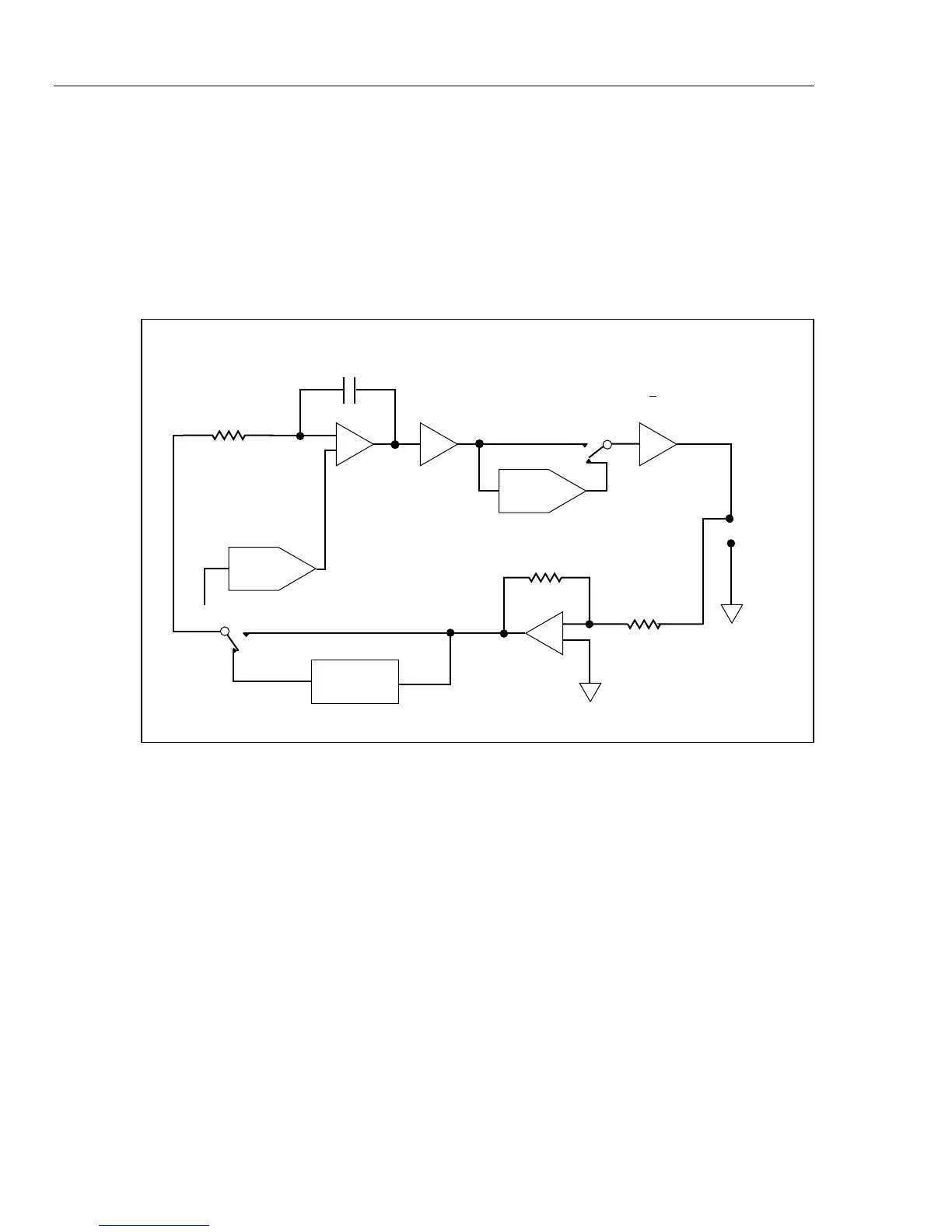
Figure 6 is a block diagram of the voltage function and shows the signal paths for
dc and ac voltage outputs. The DAC shown in the figure is VDAC, which resides
on the DDS PCA. Note that the voltage amplifier for outputs ≥3.3 V resides on
the Voltage PCA, but the amplifier for voltage outputs <3.3 V is on the DDS PCA.
+
_
+
_
VDAC
Error
Amp
DDS
AC
Converter
SCOM
SCOM
Voltage
Amp
( > 3.3V on A8,
< 3.3V on A6 )
Ref
ac
dc
Sense
Amp
dc
ac
±G
± 1
NORMAL
HI
NORMAL
LO
yg120f.eps
Figure 6. Voltage Function
Main CPU PCA (A9)
The Main CPU PCA (A9) attached to the rear-panel assembly communicates
with:
• Inguard CPU on the DDS PCA (A6)
• Display assembly CPU
• Serial interfaces
The main CPU memory is Flash ROM. There is a real-time clock with a battery
backup.
The CPU PCA communicates with each of the analog PCAs via a digital bus.
Each analog assembly has the same bus structure:
• One or more Chip Select lines
• Common data bus that connects to the motherboard, latched in by latches
• A fault line that sets all modules to a safe condition if a malfunction is found
The routing of signals to the front panel jacks are controlled by output relays on
the motherboard.