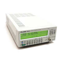
Voltage limiter
A voltage limiter that protects the impedance converter against
overvoltage is placed between the attenuator and the impedance con
-
verter. The voltage limiter consists of resistor R35 and the diodes D1
and D3 to clamp positive voltage and resistor R36 plus the diodes D2
and D4 to clamp negative voltage. The clamp voltage is approxi
-
mately ±2.1 V for low frequency signals. At high frequency the
clamp voltage rises to approximately ±2.3 V.
n
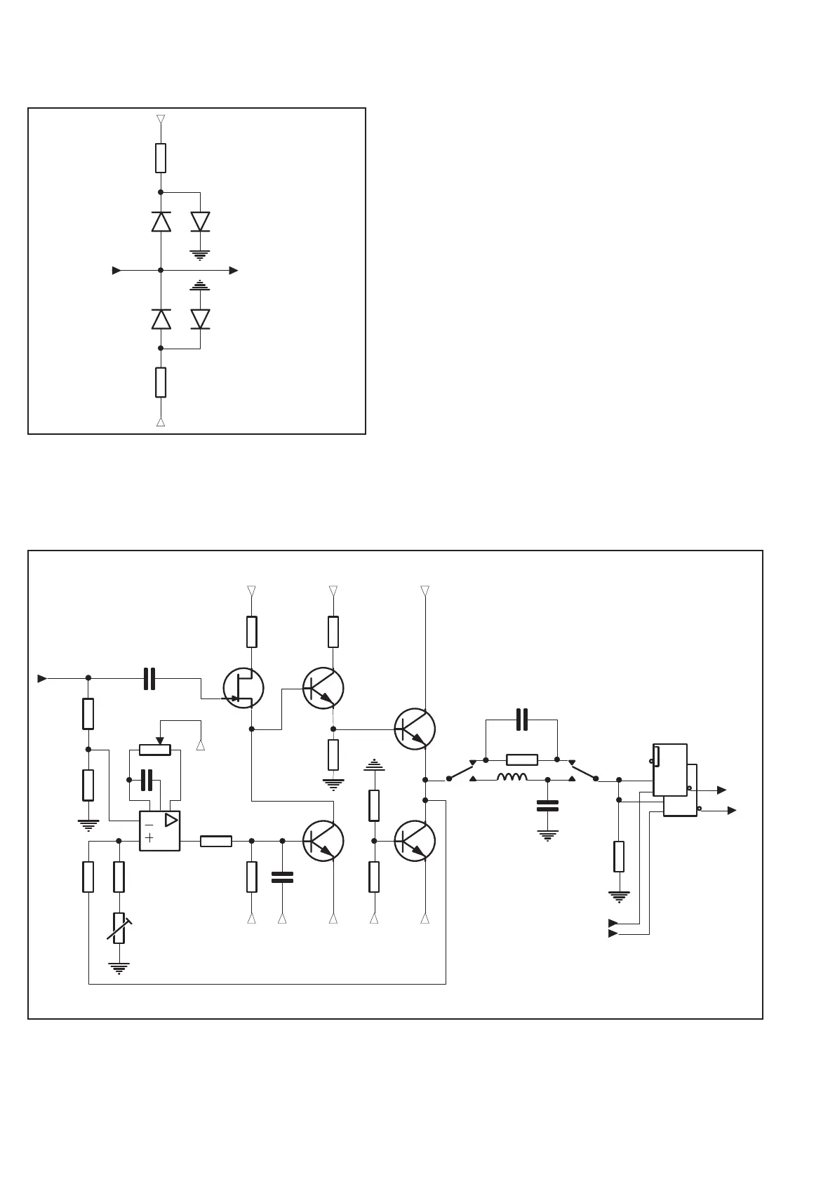
Impedance Converter Stage
The analog signal from the input stage is fed to an amplifier stage
where split-band technique is used to get good frequency response
over a wide range. This means that the high-frequency contents of
the signal are fed to a high-impedance AC-coupled FET transistor
stage Q1. The low-frequency contents are fed to a DC-coupled oper
-
ational amplifier stage with negative feedback from the output of the
converter stage buffer. The low-frequency path handles frequencies
up to approximately 5 kHz.
The high-frequency signal is fed to the gate of Q1. The high imped
-
ance at the gate is converted to a low impedance at the source. The
source is connected to the base of HF transistor Q2, the summing
point for the two signal paths.
To make the FET work well in its active region within the whole dy
-
namic range, the FET drain is supplied with +7 V via resistor R42.
The low-frequency signal is divided by the two resistors R27 and
R28 before it is coupled to the input pin #2 of the operational ampli
-
fier U1. The resistors R37 and R38 at the operational amplifier out
-
put pin #6 center the output swing, and capacitor C6 stabilizes the
operational amplifier stage.
The low-frequency path goes from the operational amplifier to the
base of transistor Q3, the collector of which is connected to the base
4-6 Hardware Functional Description
R35
D3D1
D4
D2
R36
+5
-
From
Attenuator
To Impedance
converter stage
Fig. 4-6 Voltage limiter.
Trig
Level
+
-
Q1
Q3
Q13
Q4U1
U8
C6
L1
K4
R31
R27
R28
R33
R37
R32
R38
R50
R29-
R30
-5.2 -5.2 -5.2 -5.2 -5.2
+7 +5
-5.2
Fr om Pro t ec t io n
ci rcuits
R106
C18-
C19
+5
Q2
To
Flip-Flo
+
-
R42 R43
R105
C20
C13
R46
R47
K4
C5
Fig. 4-7 Impedance converter.