Main Board
Introduction
Components not necessary for explaining the function are omitted
from the figures in this chapter. For the complete set of components,
see the circuit diagrams in Chapter 8, Drawings and Diagrams.
Input Amplifier
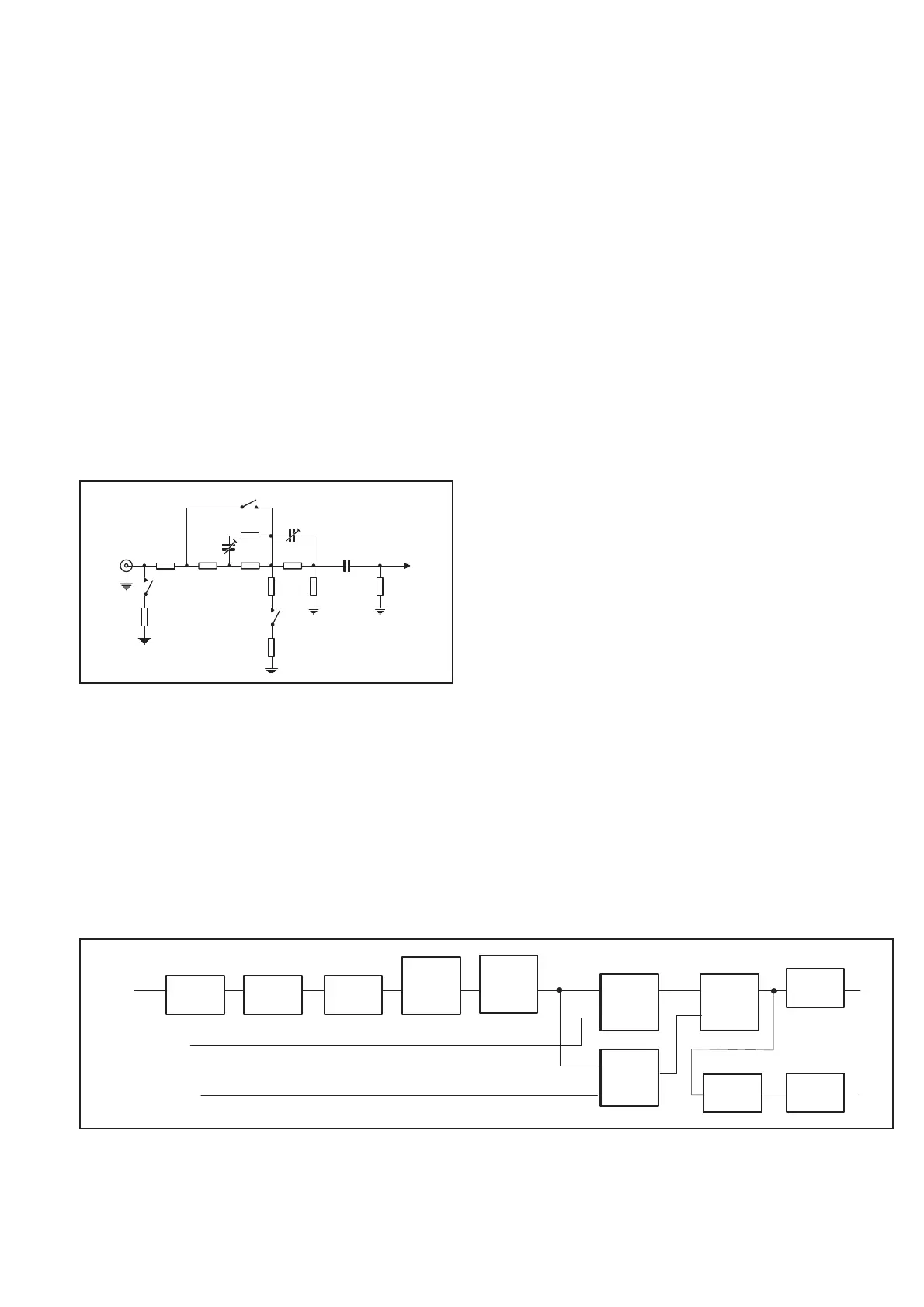
The input amplifier has 300 MHz bandwidth and is of the split-band
type. It contains four main stages: the signal adaptation stage, the im
-
pedance converter stage, the comparator stage, and the buffer stage.
n
Signal Adaptation
This part of the amplifier contains:
–
50 W/1 MW impedance selector
–
x1/x11 attenuator
–
Voltage limiter
50 W /1MW Impedance Selector
The 50 Wor1MW impedance modes are selected by relay K1. 50 W
is selected via the resistors R7 to R17, if the relay is closed. 1 MW is
selected if the relay is open. Depending on selected attenuation, the
1MW input impedance is determined by different combinations of
resistors.
In x1 attenuation mode (K2 is closed and K3 is open) the impedance
is determined by resistor network R22 to R28.
In x11 attenuation mode (K2 is open and K3 is closed) the same net
-
work as in the x1 case is involved plus the resistors R3 to R5 and R18
to R20.
The input capacitance in parallel with 1 MW is 24 pF at x1 attenua
-
tion and 12 pF at x11 attenuation.
The series resistor R1 immediately after the selector serves both as
current limiter together with the voltage limiter (see below) and as
impedance matching resistor. The resistor also improves the Volt
-
age-Standing-Wave-Ratio (VSWR) of the amplifier input.
x1/x11 Attenuator
The x1 attenuator consists of a resistive low-frequency divider,
which reduces the input signal by a factor of 2, and a capacitive
high-frequency divider. The attenuator is formed by the resistors
R22-R23 and R24-R26 in parallel with R27-R28. The capacitive part
is formed by the variable capacitor C2 in parallel with R22-R23, and
the parasitic capacitance across R24-R26.
The capacitive attenuator is adjusted via variable capacitor C2 to the
same attenuation value as the resistive attenuator.
The x11 attenuator also consists of a resistive low-frequency divider
and a capacitive high-frequency divider. The resistive part is formed
by R1-R5, and R18-R20 in parallel with 1 MW (the x1 attenuator im
-
pedance). The capacitive divider is formed by the variable capacitor
C1 and the parasitic capacitance at the node where R5, R18 and R22
meet.
Resistors R2 and R6 improve the frequency response.
Hardware Functional Description 4-5
K1
K2
K3
R6
J1
C3
R1
R2 R3-R5
R19-
R20
R18
C2
R24-
R26
R22-R23
To Voltage
li mi ter
R7-R17
C1
R27-
R28
Fig. 4-4 Impedance selector and 1X/11X attenuator.
Imp. Att. Limiter
Imp.
Conv.
Comp-
arator
Input A
A
LP
filter
Trigger
level Comp I
Comp-
arator
Trigger
level Comp II
Buffer
Flip-
Flop
Buffer
÷2
A2
Fig. 4-5 Input amplifier block diagram.