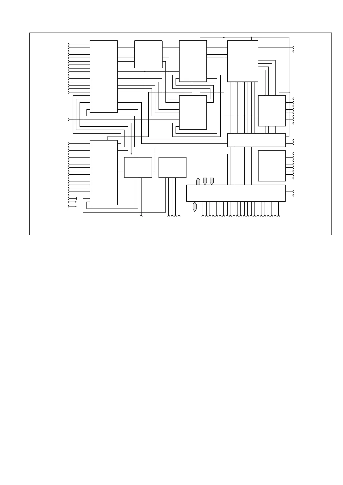
CNTS
Two 32-bit binary counters count external events or keep track of the
time.
Interpolator
This block is not used at present.
MCTRL
The different events in the measurement cycle of the ASIC are timed
by this block.
MPI
This is the microprocessor interface block. The bus width is 16 bits,
AD0 to AD15. Interrupts to the microprocessor are generated at INT.
GET
The GET signal from an optional GPIB interface can control the start
of a measurement.
n
External Interpolator
The X-POLATOR unit is connected directly to the internal
interpolator in the ASIC. It is used for increasing the time resolution
beyond the limits set by the reference clock period of 100 ns. An er
-
ror pulse is generated in the SYNC block. Its width is determined by
the difference between an external event on an input channel and the
next clock pulse. This pulse controls a current generator charging a
capacitor. When the pulse has expired the voltage across the capaci
-
tor is A/D converted and the value is added to the result. There are
two interpolators, one for the start event and one for the stop event.
They are calibrated over the possible error pulse range to allow for
any aberrations from the theoretical linear behavior.
Oscillator Circuits
n
CPU Oscillator
The microcontroller U11 is clocked at 12 MHz. The crystal B1 is
connected to the XTAL inputs of the microcontroller.
n
Reference Oscillators
A 10 MHz crystal oscillator is used as the reference for the measur
-
ing logic. If a stable external 10 MHz reference is available, it can be
connected to REF IN on the rear panel and selected by means of the
EXT REF button on the front panel.
In addition to the standard crystal oscillator there are two optional
oven-controlled crystal oscillators (OCXO) to choose from.
Standard
The uncompensated standard oscillator consists of the crystal B2,
C109, C113-C115, R209 and R211. C115 is used for manual adjust
-
ment of the frequency when the calibration tolerance has been ex
-
ceeded. The active circuitry is built into the ASIC U29 and is accessi
-
ble via the pins marked X1 and X2.
OCXO
If one of the OCXOs is mounted, the standard oscillator has to be in
-
activated by moving the jumpers J23 and J25 to their alternative po
-
sition. These oscillators are connected to J24 and are self-contained
Hardware Functional Description 4-11
FI N 1
MUX HO SYNC CNTS
STST
Inter-
polator
MCTRL
TLDAC
RTC
PG
OSC
MPI
A2
A
SR
B
B2
EXTC
P
BURST
TRA
TRB
VCCO
GNDD1
GNDD2
GNDD3
GNDD4
GET
X1
X2
V+R EFO
OTRIM
V- R EFO
EXTREF
MTC XO
IN TR EF
OUTMUX
MPCLK
PH1
PH2
VCCB
GNDB
VCCC
GNDC
GNDA
VCCA
+5
PGARM
MREF
FREQC
TI ME
MCLK
RE SET
CY 1
CY 2
VC CG
GNDG
VR EFA D
IR ES
IN TP1
IN TP2
IN TS1
IN TS2
FIN
MTIM E
V+R EFA
VOU TA
V- RE FA
V+R EFB
VOU TB
V- RE FB
VC CE
GNDE
VC CF
GNDF
X
Y
XH
YH
HO S X
HO S Y
CL O C K
STOP
START
GATEO
R1
R2
L1
L2
S TAARM
STOARM
STADL Y
STODL Y
TOTSTA
STA
INTB
INTA
SB
SA
I
FNa
I
FNb
OK a
OKb
PCL
OK
DMAR
DMABR
CS RS SS
PGTRIG
PGR EF
PGOUT
PGTRIG
PGA RM
MCLK
MCLK
PGOUT
CLOCK
STA ARM
STOA RM
STA DL Y
STODL Y
HO S X
HO S Y
GET
TOTSTA
STA
FRE QC
TI ME
MREF
RTC
RTC
R1
R2
L1
L2
XH
YH
X
Y
PCL
ST OP
ST AR T
HODLYX
HODLYY
I
FNA
F
I
NB
I
FNC
I
FND
OKA
OKB
OK C
OKD
PG
RTCX1
RTCX2
LARMN
VBAT
AD0-AD15
ALE
RDN
WRHN
WR L N
CS
A16
A17
A18
A19
HO L D N
HLDAN
QDM AN
INT
S1N
S2N
S3N
S4N
S5N
C1
C2
C3
C4
HODLYX
HODLYY
CLOCK
PGR EF
VCCX +5
Fig. 4-11 Counter ASIC, block diagram.