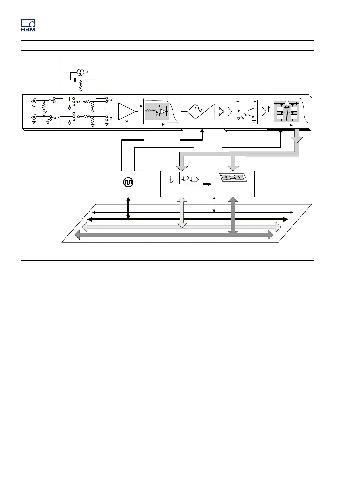
Block Diagram
Communication
& Memory &
Recording control
1.0 or 1.024 MHz
Backplane
1010
AC/DC/GND
Channel 1 to 4
Amplifier Analog Anti-Alias Filter
ADC
Digital Filter &
Sample Rate selection
System Trigger Bus
Communication and
Data
Streaming
Acquisition Control
Master Time Base
F
A
Sample Rate
+
-
Synchronization
& Sample Rate
1.0 or 1.024 MHz
Channel &
Card Trigger
T
F
n
-1
n
-1
z
-1
z
-1
Σ
a
1
a
2
b
2
b
1
x
(n)
y
(n)
A
Isolation
Current
IEPE
Us
Figure A.78: Block Diagram
Note The
specifications listed are valid for cards that have been calibrated and are used in the same mainframe and
slots as they were at the time of calibration. When the card is removed from its original location and placed in
another slot and/or mainframe, the Offset error, Gain error and MSE specifications are expected to increase
(up to double the original specification) due to thermal differences within the configurations. All specifications
are defined at 23 °C
±
2 °C, unless specified differently.
GEN3i
482 I3763-3.1 en HBM: public
 Loading...