Service Manual
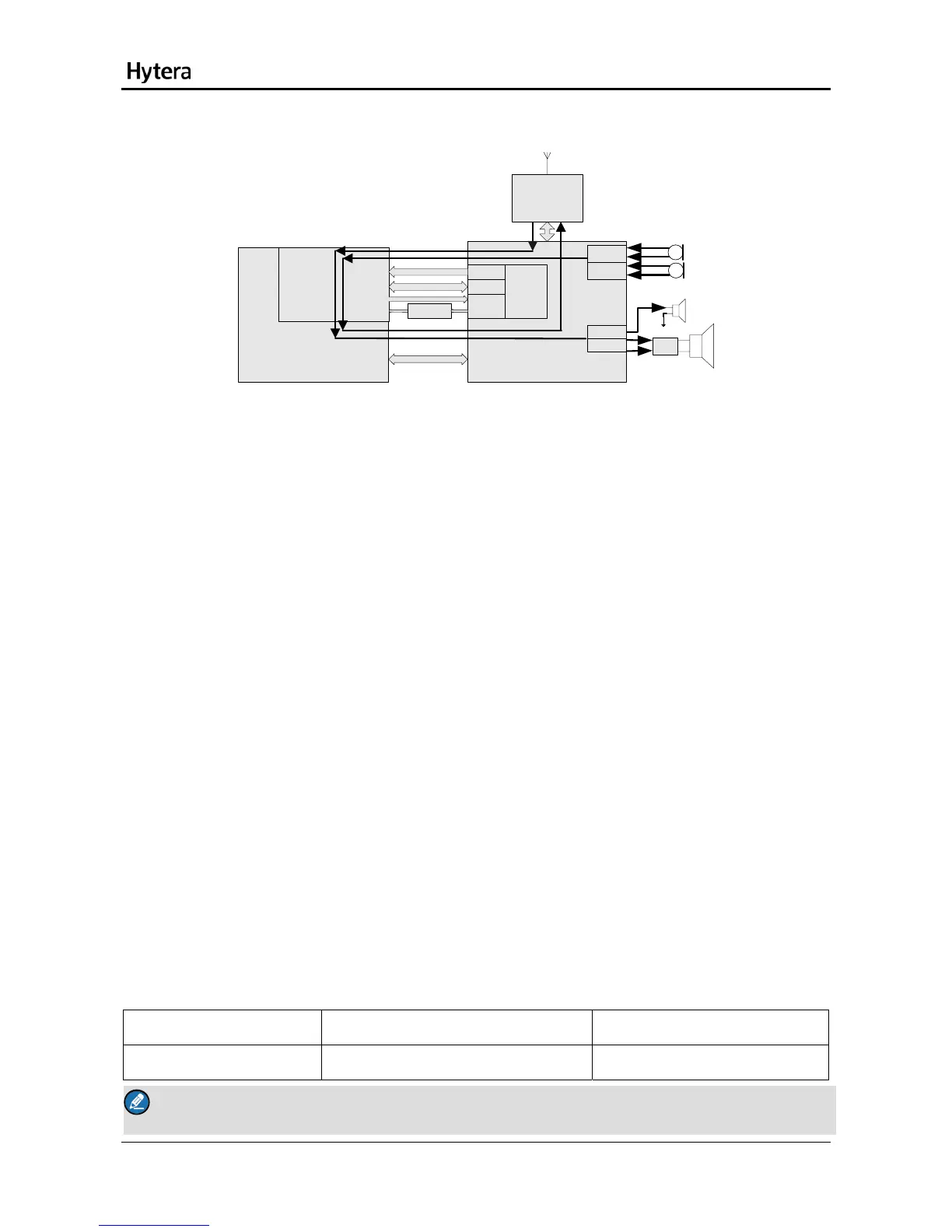
2.3 Audio Section
MCBSP 1
MCBSP 3
MCBSP 2
FSB3
FSB1
FSB2
RF
CLOCK
IRQ
RESET
IRQ
RESET
CLOCK
MIC1
MIC2
AUD
EAR
PA
CODEC
MCU
DSP
I/Q
FPGA
b
Baseband
Processor
Figure 15 Diagram of Audio Processing Circuit
2.3.1 Audio input
The audio signal from the MIC goes to the baseband processor for amplification, A/D conversion,
encoding and filtering. After such processing, the PCM code is generated, and is then sent to the MCU
for voice encoding and channel encoding by the DSP. After that, it is converted to I/Q signal by the
baseband processor via π/4 DQPSK modulation, filtering and D/A conversion. Finally, the I/Q signal is
sent via the antenna after modulation, amplification and filtering.
2.3.2 Audio output
The RF signal passes through the antenna, LNA, mixer, filter, IF amplifier and demodulator. After
demodulation, the I/Q signal is sent to the baseband processor for A/D conversion and filtering, and then
enters the MCU via the serial port. After π/4 DQPSK demodulation, channel decoding, voice decoding
by the MCU, the signal is converted to audio signal by the baseband processor via filtering and D/A
conversion. Then the audio signal goes to the audio amplifier. After amplification, the audio can drive the
speaker (the audio can be heard from an earpiece if the analog switch is connected with the accessory
jack). The signal from the receiver (duplex) is output by the baseband processor directly (not passing
through the audio amplifier).
2.3.3 Audio Amplifier Output
Main parameters are listed in the table below:
Rated Power (P
o
) 1W
R
L
= 4