Service Manual
T
R
LNA
IF Amplifier
IF BPF
Mixer
Diplexer
ANT
BPF BPF
Buffer
Demodulator
LPF
LPF
Rx_LO1
Rx_LO2
Rx PLL
IQ Processor
ANT Switch
GPS
TX
3V_Rx
RX I+
RX I-
RX Q+
RX Q-
AGC
RX
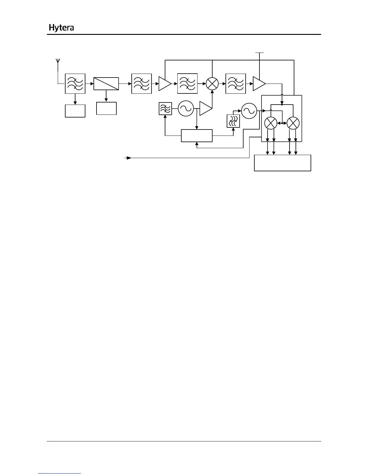
Figure 3 Diagram of RX Circuit
The working principle of the RX circuit is described below:
The RX signals pass through the RF switch. First, they are filtered to remove out-of-band signals. Then
they are amplified by the LNA and filtered again. After that, the signals are sent to the mixer for
appropriate processing. The signals output from the mixer are processed by the IF low-noise amplifier
and then by the IF filter to select desired IF signals for demodulation. The obtained I/Q signals are
filtered and finally sent to the baseband for processing.
The interfaces between the RX circuit and the baseband or other circuits are described below.
(1) 3V_RX
This interface is used to transfer the receiver on/off signal from the baseband. If the signal is at high level,
the receiver is on and the RX channel works.
(2) RX
This interface is used to transfer the RX signal output by the antenna switch of the PA.
(3) RX_LO1
This interface is used to transfer the first RX LO signal output by the VCO.
(4) RX_LO2
This interface is used to transfer the second RX LO signal (level: -10dBm) output by the VCO. The signal
enters the IF demodulator, where it is divided and then demodulated together with the first RX IF signal.
(5) AGC
The AGC control voltage from the baseband enters via this interface, to stabilize output of the I/Q
7