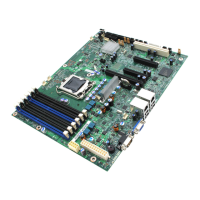
Connector/Header Locations and Pin-outs Intel® Server Board S3420GP TPS
Revision 2.4
Intel order number E65697-010
82
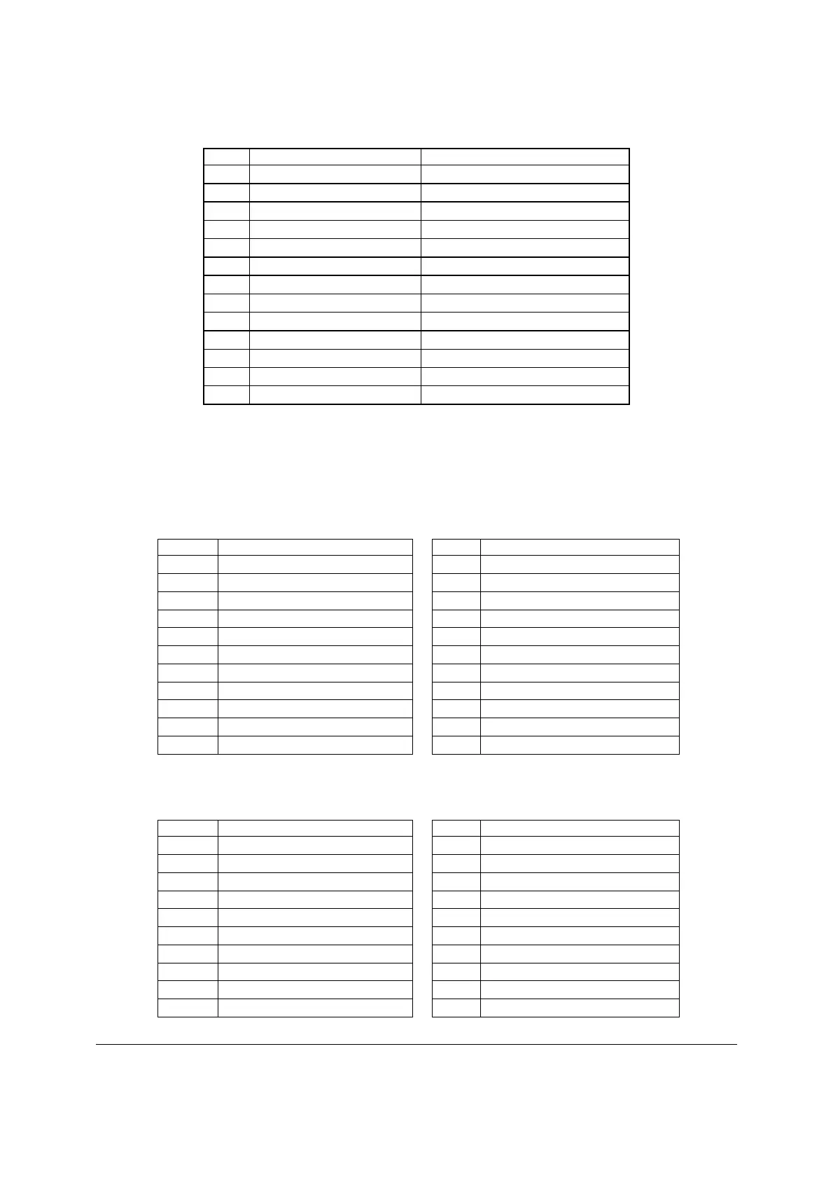
Pin Signal Name
Description
3 V_IO_B_CONN Blue (analog color signal B)
4 TP_VID_CONN_B4 No connection
5 GND Ground
6 GND Ground
7 GND Ground
8 GND Ground
9 TP_VID_CONN_B9 No connection
10 GND Ground
11 TP_VID_CONN_B11 No connection
12 V_IO_DDCDAT DDCDAT
13 V_IO_HSYNC_CONN HSYNC (horizontal sync)
14 V_IO_VSYNC_CONN VSYNC (vertical sync)
15 V_IO_DDCCLK DDCCLK
7.5.2 Rear NIC and USB connector
The server board provides two stacked RJ-45/2xUSB connectors side-by-side on the back edge
of the board (J6A1, J5A1). The pin-out for NIC connectors are identical and defined in the
following table.
Table 48. RJ-45 10/100/1000 NIC Connector Pin-out (J5A1)
Pin Signal Name
Pin Signal Name
1 P5V_USB_PWR75 2 USB_PCH_11_FB_DN
3 USB_PCH_11_FB_DP 4 GND
5 P5V_USB_PWR75 6 USB_PCH_10_FB_DN
7 USB_PCH_10_FB_DP 8 GND
9 P1V9_LAN2_R 10 NIC2_MDIP<0>
11 NIC2_MDIN<0> 12 NIC2_MDIP<1>
13 NIC2_MDIN<1> 14 NIC2_MDIP<2>
15 NIC2_MDIN<2> 16 NIC2_MDIP<3>
17 NIC2_MDIN<3> 18 GND
19 LED_NIC2_1 20 P3V3_AUX
21 LED_NIC2_LINK100_R_0 22 LED_NIC2_LINK1000_2
Table 49. RJ-45 10/100/1000 NIC Connector Pin-out (J6A1)
Pin Signal Name
Pin Signal Name
1 P5V_USB_PWR75 2 USB_PCH_11_FB_DN
3 USB_PCH_11_FB_DP 4 GND
5 P5V_USB_PWR75 6 USB_PCH_10_FB_DN
7 USB_PCH_10_FB_DP 8 GND
9 P1V8_PHY_VCT_R 10 NIC1_MDIP<0>
11 NIC1_MDIN<0> 12 NIC1_MDIP<1>
13 NIC1_MDIN<1> 14 NIC2_MDIP<2>
15 NIC1_MDIN<2> 16 NIC2_MDIP<3>
17 NIC1_MDIN<3> 18 GND
19 LED_NIC1_LINK_ACT_0_R 20 P3V3_AUX
 Loading...