2FT
2-3-11
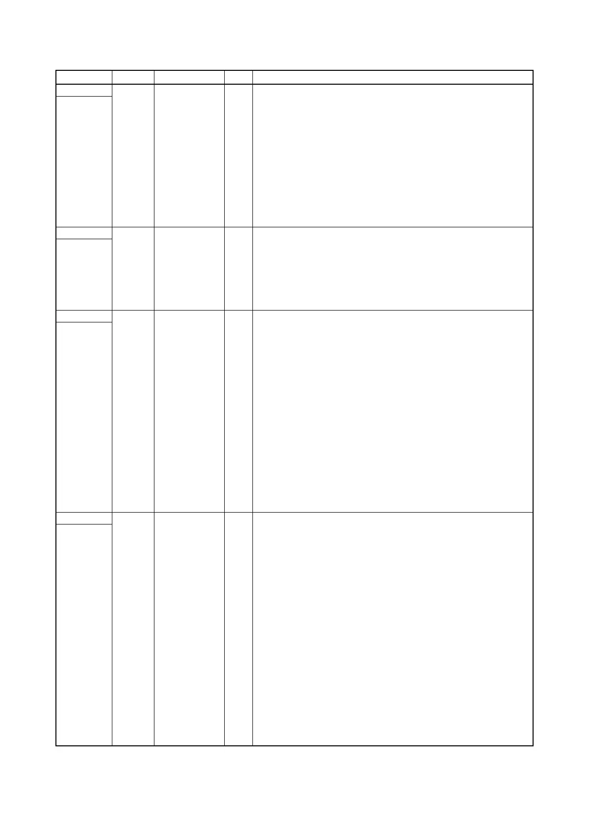
YC6 1 ORGTIMN I DP original scanning interval signal
Connected
to the DP*
2 DOPRDY I DP READY signal
3 DOPSEL O DP SELECT signal
4 SGND - Ground
5 DOPCLK O DP clock signal
6 DOPSDI I DP serial communication reception
7 DOPSDO O DP serial communication transmission
8 +5V4 O 5 V DC power supply for DP
9 PGND - Ground
10 PGND - Ground
11 +24V1 O 24 V DC power supply for DP
12 +24V1 O 24 V DC power supply for DP
YC7 1 +24V4 O 24 V DC power supply for DM
Connected
to the drive
motor
2 PGND - Ground
3 SGND - Ground
4 +5V O 5 V DC power supply for DM
5REM ODM on/off
6 RDY I DM rotation sync signal
7 CLK O DM clock signal
YC8 1 BPPESW I BYPPSW on/off
Connected
to the
drawer PCB
2 C1PDSWN I PSW on/off
3 FCLTN O PFCL on/off
4 +24V1 O 24 V DC power supply for DPCB
5 BPSOLN O BYPPFCL on/off
6 ICLTN O DUPFCL on/off
7 IPPSWN I DUPPCSW on/off
8 BPWSW I BYPPWSW on/off
9 REGSWN I RSW on/off
10 TONEPY I TCS on/off
11 SGND - Ground
12 +5V2 O 5 V DC power supply for DPCB
13 C1PWSWN I PWSW on/off
14 HUMIDC I HUMSENS analog signal
15 HMCLK2 O HUMSENS clock signal (2)
16 HMCLK1 O HUMSENS clock signal (1)
17 TEMP I HUMSENS analog signal
YC9 1 HVCLK O Developing bias clock signal
Connected
to the high-
voltage PCB
2 +5V O 5 V DC power supply for HVTPCB
3 SHVISELN O Separation high-voltage switch signal
4 PGND - Ground
5 MHVDRN O Main charging high-voltage on/off
6 PGND - Ground
7 SHVDRN O Separation high-voltage on/off
8 PGND - Ground
9 MHVADJ O Main charging high-voltage adjust signal
10 PGND - Ground
11 THVDRN O Transfer high-voltage on/off
12 +24V4 O 24 V DC power supply for HVTPCB
13 THVADJ O Transfer high-voltage adjust signal
14 +24V4 O 24 V DC power supply for HVTPCB
15 PGND - Ground
16 +24V4 O 24 V DC power supply for HVTPCB
*: Optional.
Connector Pin No. Signal I/O Description

 Loading...