170
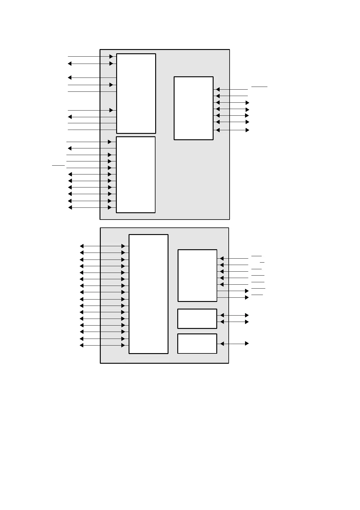
Q701 : TMS320DA610A003BPYP225
TRST
GP0[7](EXT_INT7)
§#
IEEE Standard
1149.1
(JTAG)
Emulation
Reset and
Interrupts
Control/Status
TDI
TDO
TMS
TCK
EMU0
EMU1
NMI
GP0[6](EXT_INT6)
§#
GP0[5](EXT_INT5)/AMUTEIN0
§
GP0[4](EXT_INT4)/AMUTEIN1
§
RESET
Clock/PLL
Oscillator
CLKIN
CLKMODE0
CLKOUT2/GP0[2]
EMU2
†
EMU3
†
EMU4
†
EMU5
†
OSCIN
OSCOUT
HHWIL/AFSR1
HCNTL0/AXR0[12]/AXR1[3]
HCNTL1/AXR0[14]/AXR1[1]
Data
Register Select
Half-Word
Select
Control
HPI
(Host-Port Interface)
HAS
/ACLKX1
HR/W
/AXR0[15]/AXR1[0]
HCS
/AXR0[13]/AXR1[2]
HDS1
/AXR0[9]/AXR1[6]
HDS2
/AXR0[10]/AXR1[5]
HRDY
/ACLKR1
HINT
/GP0[1]
HD15/GP0[15]
HD14/GP0[14]
HD13/GP0[13]
HD12/GP0[12]
HD11/GP0[11]
HD10/GP0[10]
HD9/GP0[9]
HD8/GP0[8]
HD7/GP0[3]
HD6/AHCLKR1
HD5/AHCLKX1
HD4/GP0[0]
HD3/AMUTE1
HD2/AFSX1
HD1/AXR0[8]/AXR1[7]
HD0/AXR0[11]/AXR1[4]
CLKOUT3
HD4/GP0[0]
§
PLLHV
OSCV
DD
OSCV
SS
†
These external pins are applicable to the GDP package only.
‡
The GP0[15:0] pins, through interrupt sharing, are external interrupt capable via GP0INT0. For more detail, see the external interrupt
section of this data sheet. For more detail on interrupt sharing, see the TMS320C6000 DSP Interrupt Selector Reference Guide
(literature number SPRU646).
§
All of these pins are external interrupt sources. For more detail, see the external interrupt sources section of this data sheet.