174
cles in Single Speed, 2304 cycles in Double Speed and 4608 cycles in Quad Speed mode. The bias volt-
age on the outputs will be retained and MUTEC
will go active at the completion of the ramp period.
The analog outputs will ramp to a normal state when this function transitions from the enabled to disabled
state. The ramp requires 1152 left/right clock cycles in Single Speed, 2304 cycles in Double Speed and
4608 cycles in Quad Speed mode. The MUTEC
will release immediately on setting MUTE = 1.
The converter analog outputs will mute when enabled. The bias voltage on the outputs will be retained
and MUTEC
will go active during the mute period.
Control Port / Hardware Mode Select - C/H
Pin 16, Input
Function:
Determines if the device will operate in either the Hardware Mode or Control Port Mode.
Mute Control - MUTEC
Pin 17, Output
Function:
The
Mute Control pin goes low during power-up initialization, reset, muting, master clock to left/right clock
frequency ratio is incorrect or power-down. This pin is intended to be used as a control for an external mute
circuit to prevent the clicks and pops that can occur in any single supply system. Use of Mute Control is not
mandatory but recommended for designs requiring the absolute minimum in extraneous clicks
and pops.
Analog Ground - AGND
Pins 18 and 21, Inputs
Function:
Analog ground reference.
Differential Analog Outpus - AOUTR- , AOUTR+ and AOUTL- , AOUTL+
Pins 19, 20, 23 and 24, Outputs
Function:
The full scale differential analog output level is specified in the Analog Characteristics specifications table.
Analog Power - VA
Pin 22, Input
Function:
Power for the analog and reference circuits. Typically 5VDC.
Mute
DESCRIPTION
0
Enabled
1
Normal operation mode
C/H
DESCRIPTION
0
Hardware Mode Enabled
1
Control Port Mode Enabled
Common Mode Voltage - CMOUT
Pin 25, Output
Function:
Filter connection for internal bias voltage, typically 50% of VREF. Capacitors must be connected from
CMOUT to analog ground, as shown in Figure 6. CMOUT has a typical source impedence of 25 k
Ω
and
any current drawn from this pin will alter device performance
Reference Ground - FILT-
Pin 26, Input
Function:
Ground reference for the internal sampling circuits. Must be connected to analog ground.
Reference Filter - FILT+
Pin 27, Output
Function:
Positive reference for internal sampling circuits. External capacitors are required from FILT+ to analog
ground, as shown in Figure 6. The recommended values will typically provide 60 dB of PSRR at 1 kHz
and 40 dB of PSRR at 120 Hz. FILT+ is not intended to supply external current.
Voltage Reference Input- VREF
Pin 28, Input
Function:
Analog voltage reference. Typically 5VDC.
HARDWARE MODE
Mode Select - M0, M1, M2, M3, M4
Pins 2, 3, 4, 5 and 14, Inputs
Function:
The Mode Select pins determine the operational mode of the device as detailed in Tables 9-14. The op-
tions include;
Selection of the Digital Interface Format which determines the required relationship between the
Left/Right clock, serial clock and serial data as detailed in Figures 29-33
Selection of the standard 15
μ
s/50
μ
s digital de-emphasis filter response, Figure 28, which requires re-
configuration of the digital filter to maintain the proper filter response for 32, 44.1 or 48 kHz sample rates.
Selection of the appropriate clocking mode to match the input sample rates.
Access to the Direct Stream Digital Mode
Access to the 8x Interpolation Input Mode
CONTROL PORT MODE
Address Bit 0 / Chip Select - AD0 / CS
Pin 2, Input
Function:
In I
2
C mode, AD0 is a chip address bit. CS is used to enable the control port interface in SPI mode. The
device will enter the SPI mode at anytime a high to low transition is detected on this pin. Once the device
has entered the SPI mode, it will remain until either the part is reset or undergoes a power-down cycle.
Address Bit 1 / Control Data Input - AD1/CDIN
Pin 3, Input
Function:
In I
2
C mode, AD1 is a chip address bit. CDIN is the control data input line for the control port interface in
SPI mode.
Serial Control Interface Clock - SCL/CCLK
Pin 4, Input
Function:
In I
2
C mode, SCL clocks the serial control data into or from SDA/CDOUT.
In SPI mode, CCLK clocks the serial data into AD1/CDIN and out of SDA/CDOUT.
Serial Control Data I/O - SDA/CDOUT
Pin 5, Input/Output
Function:
In I
2
C mode, SDA is a data input/output. CDOUT is the control data output for the control port interface in
SPI mode.
M1 - Mode Select
Pin 14, Input
Function:
This pin is not used in Control Port Mode and must be terminated to ground.
5.0 PIN DESCRIPTION - DSD MODE
Master Clock - MCLK
Pin 10, Input
Function:
The master clock frequency must be either 4x or 6x the DSD data rate for 64x oversampled DSD data
and 2x or 3x the DSD data rate for 128x oversampled DSD data, refer to Table 7.
CLKMODE
Pin 12, Input
Function:
This pin determines the allowable Master Clock to DSD data ratio as defined in Table 7.
DSD Serial Clock - DSD_SCLK
Pin 11, Input
Function:
Clocks the individual bits of the DSD audio data into the DSD_L and DSD_R pins.
Audio Data - DSD_L and DSD_R
Pins 13 and 14, Inputs
Function:
Direct Stream Digital audio data is clocked into DSD_L and DSD_R via the DSD serial clock.
CLKMODE
DSD Over-
Sampling Ratio
01
64x 4x 6x
128x 2x 3x
Table 7. MCLK to DSD Data Rate Clock Ratios
Refer to PCM mode RST VREF Refer to PCM mode
Refer to PCM mode M4(ADO/CS
) FILT+ Refer to PCM mode
Refer to PCM mode M3(AD1/CDIN) FILT- Refer to PCM mode
Refer to PCM mode M2(SCL/CCLK) CMOUT Refer to PCM mode
Refer to PCM mode M0(SDA/CDOUT) AOUTL- Refer to PCM mode
Refer to PCM mode DGND AOUTL+ Refer to PCM mode
Refer to PCM mode VD VA Refer to PCM mode
Refer to PCM mode VD AGND Refer to PCM mode
Refer to PCM mode DGND AOUTR+ Refer to PCM mode
Master Clock MCLK AOUTR- Refer to PCM mode
DSD Serial Clock DSD_SCLK AGND Refer to PCM mode
Master Clock Mode CLKMODE MUTEC
Refer to PCM mode
Left Channel Data DSD_L C/H
Refer to PCM mode
Right Channel Data DSD_R MUTE
Refer to PCM mode
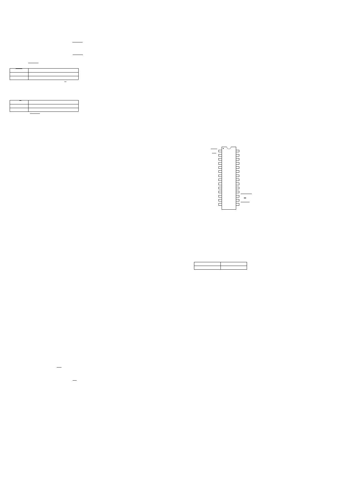
1
2
3
4
5
6
7
8
9
10
11
12
5
1
2
6
28
27
26
25
24
23
22
21
20
19
18
17
13
14
16
15
QD01, QD03, QD05, QD07 : CS4397-KSZ