171
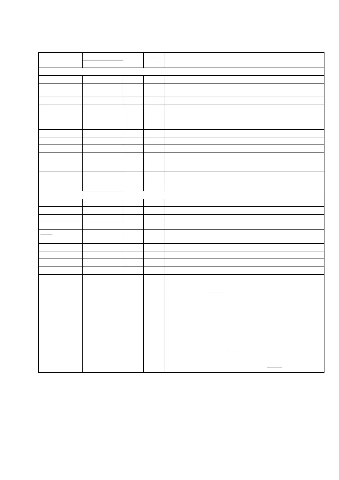
Terminal Functions
SIGNAL PIN NO.
IPD/
NAME PYP GDP
TYPE
†
IPU‡
DESCRIPTION
CLOCK/PLL CONFIGURATION
CLKIN 204 A3 I IPD Clock Input
CLKOUT2/GP0[2] 82 Y12 O/Z IPD
Clock output at half of device speed (O/Z) [default] (SYSCLK2 internal signal
from the PLL controller) or this pin can be programmed as GP0[2] pin (I/O/Z)
CLKOUT3 184 D10 O IPD Programmable clock output (OSC Divider internal signal from PLL controller)
CLKMODE0 205 C4 I IPU
PLL input clock source select
• Selects whether the PLL input clock is CLKIN (square wave) [pin high] or
whether the PLL input clock is directly from the crystal oscillator (OSCIN and
OSCOUT) [pin low].
PLLHV 202 C5 A
§
Analog power (3.3 V) for PLL
OSCIN 178 D12 I — Crystal oscillator Input (XI)
OSCOUT 179 C12 O — Crystal oscillator output (XO)
OSCV
DD
181 A12 S —
Power for crystal oscillator (1.2 V), Do not connect to board power 1.2 V; for
optimum performance, connected internally. If CLKIN is used instead of the
oscillator, then this pin can be left open or connected to CV
DD
.
OSCV
SS
180 B11 GND —
Ground for crystal oscillator, Do not connect to board ground; for optimum
performance, connected internally. If CLKIN is used instead of the oscillator,
then this pin can be left open or connected to V
SS
.
JTAG EMULATION
TMS 192 B7 I IPU JTAG test-port mode select
TDO 187 A8 O/Z IPU JTAG test-port data out
TDI 191 A7 I IPU JTAG test-port data in
TCK 193 A6 I IPU JTAG test-port clock
TRST 197 B6 I IPD
JTAG test-port reset. For IEEE 1149.1 JTAG compatibility, see the IEEE 1149.1
JTAG Compatibility Statement section of this data sheet.
EMU5 — B12 I/O/Z IPU Emulation pin 5. Reserved for future use, leave unconnected.
EMU4 — C11 I/O/Z IPU Emulation pin 4. Reserved for future use, leave unconnected.
EMU3 — B10 I/O/Z IPU Emulation pin 3. Reserved for future use, leave unconnected.
EMU2 — D3 I/O/Z IPU Emulation pin 2. Reserved for future use, leave unconnected.
EMU1
EMU0
185
186
B9
D9
I/O/Z IPU
Emulation [1:0] pins
• Select the device functional mode of operation
EMU[1:0]
Operation
00 Boundary Scan/Functional Mode (see Note)
01 Reserved
10 Reserved
11 Emulation/Functional Mode [default] (see the IEEE 1149.1
JTAG Compatibility Statement section of this data sheet)
The DSP can be placed in Functional mode when the EMU[1:0] pins are
configured for either Boundary Scan or Emulation.
Note: When the EMU[1:0] pins are configured for Boundary Scan mode, the
internal pulldown (IPD) on the TRST
signal must not be opposed in order to
operate in Functional mode.
For the Boundary Scan mode drive EMU[1:0] and RESET
pins low.
†
I = Input, O = Output, Z = High impedance, S = Supply voltage, GND = Ground
‡
IPD = Internal pulldown, IPU = Internal pullup. [These IPD/IPU signal pins feature a 13-kΩ resistor (approximate) for the IPD or 18-kΩ resistor
(approximate) for the IPU. An external pullup or pulldown resistor no greater than 4.4 kΩ and 2.0 kΩ, respectively, should be used to pull a signal
to the opposite supply rail.]
§
A = Analog signal (PLL Filter)
Q701 : TMS320DA610A003BPYP225
 Loading...