173
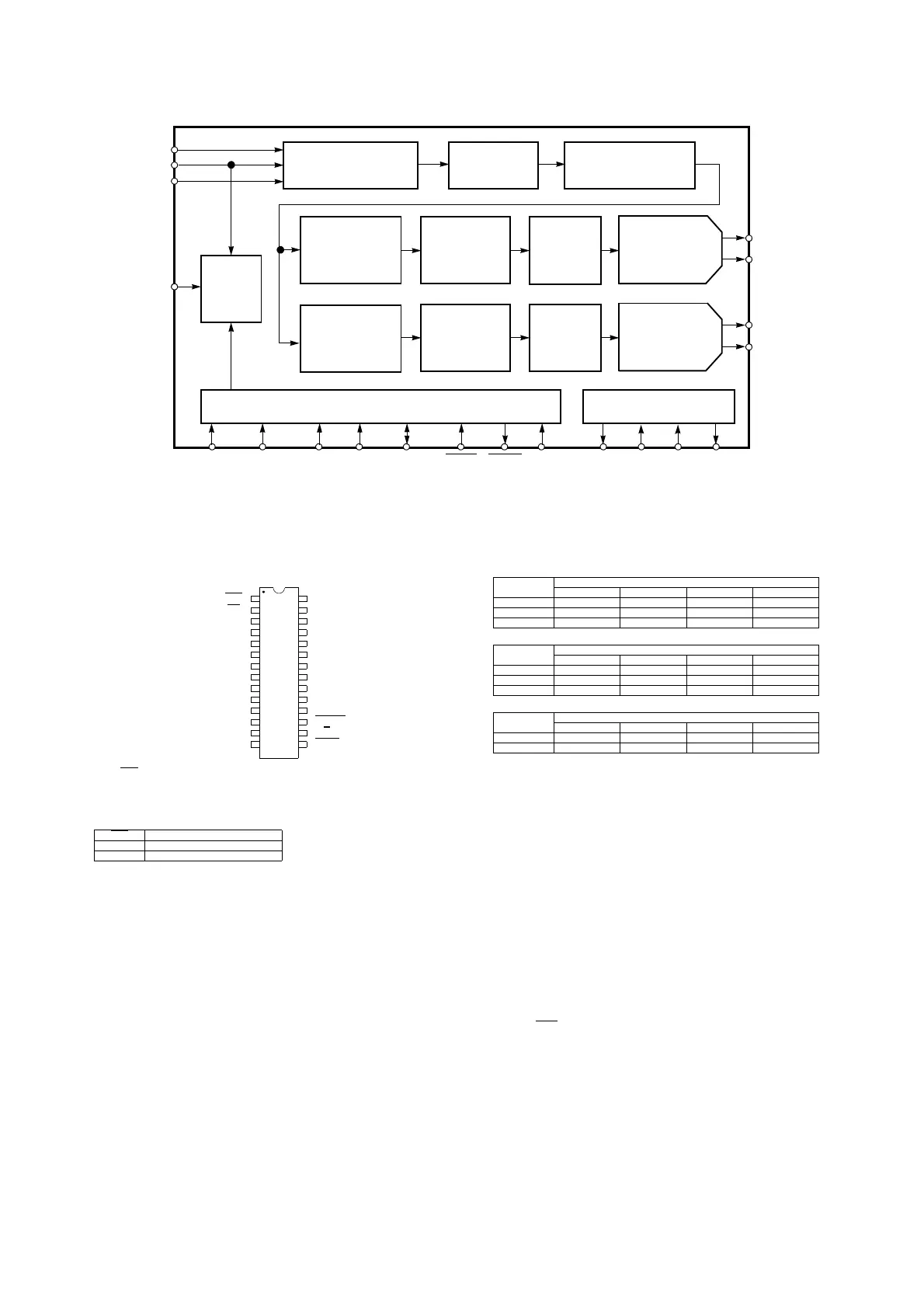
QD01, QD03, QD05, QD07 : CS4397-KSZ
SCLK
MCLK
M4
LRCK
SDATA
AOUTL+
AOUTR+
SERIAL INTERFACE
AND FORMAT SELECT
INTERPOLATION
SOFT MUTE
ΔΣ
MODULATOR
DYNAMIC
DE-EMPHASIS
SWITCHED
AOUTL-
AOUTR-
FILT+
FILTER
INTERPOLATION
FILTER
FILTER
MULTI-BIT
ΔΣ
MODULATOR
MULTI-BIT
ELEMENT
MATCHING
LOGIC
DYNAMIC
ELEMENT
MATCHING
LOGIC
CAPACITOR-DAC
AND FILTER
SWITCHED
CAPACITOR-DAC
AND FILTER
VREF CMOUTFILT-
VOLTAGE REFERENCE
HARDWARE MODE CONTROL
CLOCK
DIVIDER
(CONTROL PORT)
(AD0/CS)
M3 M2
(AD1/CDIN) (SCL/CCLK)
M1 M0
(SDA/CDOUT)
RESET MUTEC MUTE
4.0 PIN DESCRIPTION - PCM MODE
Reset - RST
Pin 1, Input
Function:
The device enters a low power mode and all internal state machines registers are reset when low. When
high, the device will be in a normal operation mode .
Digital Ground - DGND
Pins 6 and 9, Inputs
Function:
Digital ground reference.
Digital Power - VD
Pins 7 and 8, Input
Function:
Digital power supply. Typically 5.0 to 3.0 VDC.
Master Clock - MCLK
Pin 10, Input
Function:
The master clock frequency must be either 256x, 384x, 512x or 768x the input sample rate in Single
Speed Mode; either 128x, 192x 256x or 384x the input sample rate in Double Speed Mode; or 64x, 96x
128x or 192x the input sample rate in Quad Speed Mode. Tables 4-6 illustrate the standard audio sample
rates and the required master clock frequencies.
RST
DESCRIPTION
0
Enabled
1
Normal operation mode
1
2
3
4
5
6
7
8
9
10
11
12
5
1
2
6
28
27
26
25
24
23
22
21
20
19
18
17
13
14
16
15
Reset RST
VREF Voltage Reference
See Description M4(AD0/CS
) FILT+ Reference Filter
See Description M3(AD1/CDIN) FILT- Reference Ground
See Description M2(SCL/CCLK) CMOUT Common ModeS Voltage
See Description M0(SDA/CDOUT) AOUTL- Differential Output
Digital Ground DGND AOUTL+ Differential Output
Digital Power VD VA Analog Power
Digital Power VD AGND Analog Ground
Digital Ground DGND AOUTR+ Differential Output
Master Clock MCLK AOUTR- Differential Output
Serial Clock SCLK AGND Analog Ground
Left/Right Clock LRCK MUTEC
Mute Control
Serial Data SDATA C/H
Control port/Hardware select
See Description M1 MUTE
Soft Mute
Serial Clock - SCLK
Pin 11, Input
Function:
Clocks individual bits of serial data into the SDATA pin. The required relationship between the Left/Right
clock, serial clock and serial data is defined by either the Mode Control Byte in Control Port Mode or the
M0 - M4 pins in Hardware Mode. The options are detailed in Figures 29-33
Left/Right Clock - LRCK
Pin 12, Input
Function:
The Left/Right clock determines which channel is currently being input on the serial audio data input,
SDATA. The frequency of the Left/Right clock must be at the input sample rate. Audio samples in
Left/Right sample pairs will be simultaneously output from the digital-to-analog converter whereas
Right/Left pairs will exhibit a one sample period difference. The required relationship between the
Left/Right clock, serial clock and serial data is defined by the Mode Control Byte and the options are de-
tailed in Figures 29-33
Serial Audio Data - SDATA
Pin 13, Input
Function:
Two’s complement MSB-first serial data is input on this pin. The data is clocked into SDATA via the serial
clock and the channel is determined by the Left/Right clock. The required relationship between the
Left/Right clock, serial clock and serial data is defined by the Mode Control Byte and the options are de-
tailed inin Figures 29-33
Soft Mute - MUTE
Pin 15, Input
Function:
The analog outputs will ramp to a muted state when enabled. The ramp requires 1152 left/right clock cy-
Sample Rate
(kHz)
MCLK (MHz)
256x 384x 512x 768x
32 8.1920 12.2880 16.3840 24.5760
44.1 11.2896 16.9344 22.5792 33.8688
48 12.2880 18.4320 24.5760 36.8640
Table 4. Single Speed (16 to 50 kHz sample rates) Common Clock Frequencies
Sample Rate
(kHz)
MCLK (MHz)
128x 192x 256x 384x
64 8.1920 12.2880 16.3840 24.5760
88.2 11.2896 16.9344 22.5792 33.8688
96 12.2880 18.4320 24.5760 36.8640
Table 5. Double Speed (50 to 100 kHz sample rates) Common Clock Frequencies
Sample Rate
(kHz)
MCLK (MHz)
64x 96x 128x 192x
176.4 11.2896 16.9344 22.5792 33.8688
192 12.2880 18.4320 24.5760 36.8640
Table 6. Quad Speed (100 to 200 kHz sample rates) Common Clock Frequencies