Display
Jetson AGX Xavier Series Product DG-09840-001_v2.5 | 73
Parameter Requirement Units Notes
Topology Y-pattern is recommended
keep symmetry
Xtalk suppression is the best by Y-pattern.
Also it can reduce the limit of pair-pair
distance. Need
review (NEXT/FEXT check) if
via placement is not Y-pattern.
Minimum Impedance dip
Recommended via dimension for impedance
control
Drill/Pad
Antipad
Via pitch
≥97
≥92
200/400
>840
≥880
Ω @ 200ps
Ω @ 35ps
um
um
um
GND via
Place GND via as symmetrically as
possible to data pair vias. Up to 4
signal vias (2 diff pairs) can share a
single GND return via
GND via is used to maintain return path,
while its Xtalk suppression is limited
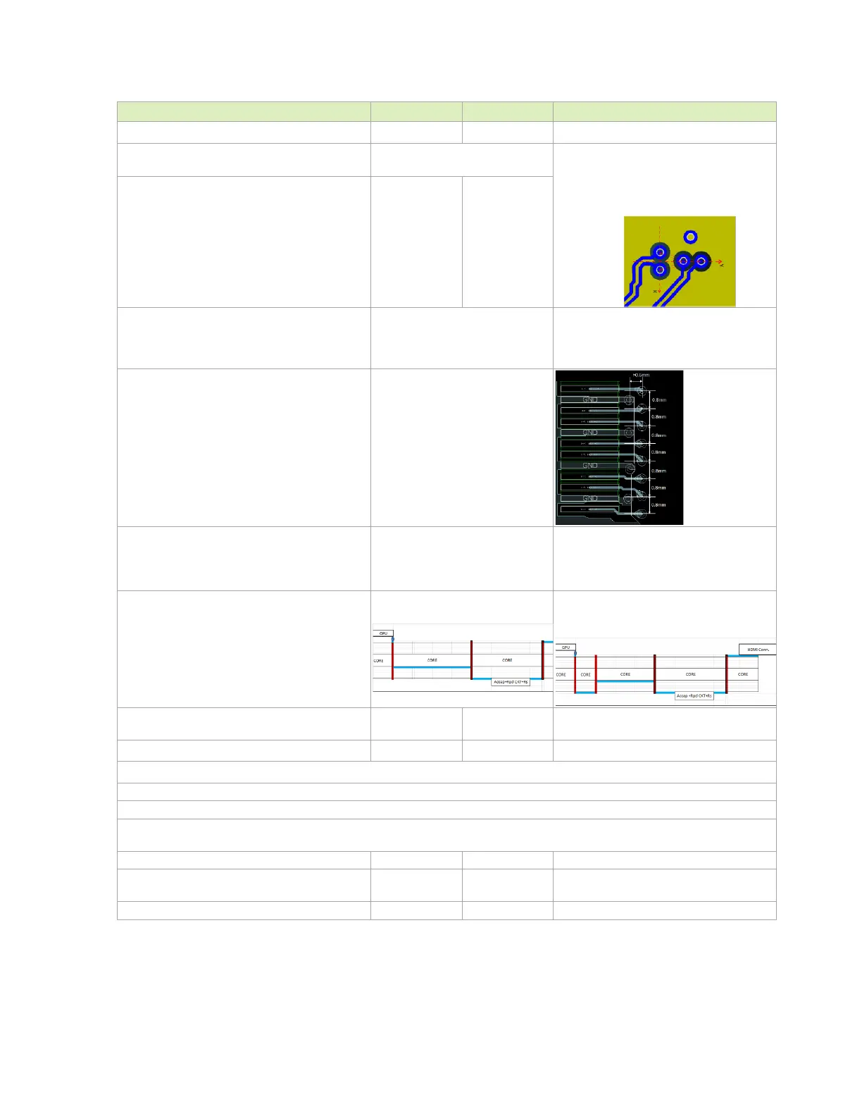
Connector pin via
The break-in trace to the connector
pin via should be routed on the
BOTTOM in order to avoid via stub
effect
Equal spacing (0.8mm) between
adjacent signal vias.
The x-axis distance between signal
and GND via should be > 0.6mm
Max # of Vias
PTH vias
Micro Vias
4 if all vias are PTH via
Not limited as long as total channel
loss meets IL spec
No breakout: ≤ 3 vias
breakout on the same layer as main trunk:
≤ 4 vias
Max Via Stub Length 0.4 mm
long via stub requires review (IL and
resonance dip check)
(See USB 3.1 Guidelines)
(See Figure 9-4)
The main-route via dimensions should comply with the via structure rules (See Via section)
For the connector pin vias, follow the rules for the connector pin vias (See Via section)
The traces after main-route via should be routed as 100Ω differential or as uncoupled 50ohm Single-ended traces on PCB Top or
Bottom.
Max distance from RPD to main trace (seg B) 1 mm
Max distance from AC cap to RPD stubbing point
(seg A)
~0 mm
Max distance between ESD and signal via 3 mm

 Loading...