Display
Jetson AGX Xavier Series Product DG-09840-001_v2.5 | 74
Parameter Requirement Units Notes
Example of a case where space is limited for
placing components.
Top
Bottom
Value 0.1 uF
Max via distance from BGA 7.62 (52.5) mm (ps)
Location
must be placed before pull-down
resistor
The distance between the AC cap and the
HDMI connector is not restricted.
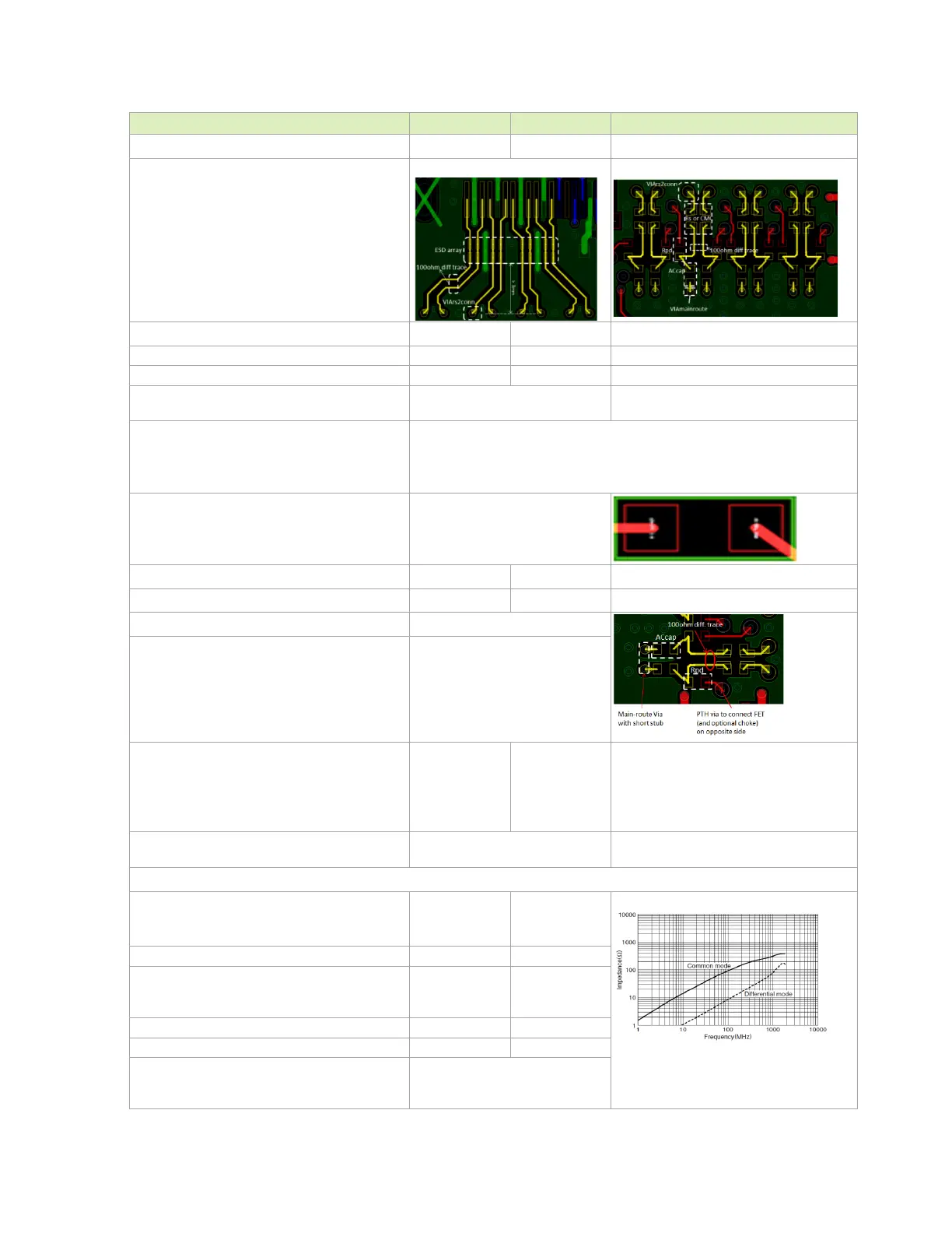
Placement
PTH design
Micro-Via design
Place cap on bottom layer if main-route above core
Place cap on top layer if main-route below core
Not Restricted
Void
GND (or PWR) void under/above the
cap is needed. Void size = SMT area
+ 1x dielectric height keepout
distance
Pull-down Resistor (RPD), choke/FET
Value
500 Ω
Location.
Must be placed after AC cap
Layer of placement
Same
layer as AC cap. The FET and
choke can be placed on the
opposite layer thru a PTH via
Choke between RPD & FET
Choke
Max Trace Rdc
Max Trace length
600 or
1
≤20
4
Ω@100MHz
uH@DC-100MHz
mΩ
mm
Can be choke or Trace. Recommended
option for HDMI2.0 HF1-9 improvement.
Void
GND/PWR void under/above cap is
preferred
(Stuffing option – not added unless EMI issue is seen)
Common-mode impedance @ 100MHz
Min
Max
65
90
Ω
TDK ACM2012D-900-2P
RDC <=0.3ohm
Differential TDR impedance
90ohm +/-15% @
Tr=200ps (10%-
90%)
Min Sdd21 @ 2.5GHz 2.22 dB
Max Scc21 @ 2.5GHz 19.2 dB
Location
Close to any adjacent discontinuity
(< 8mm) – such as connector, via,
etc.

 Loading...