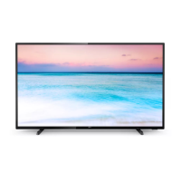
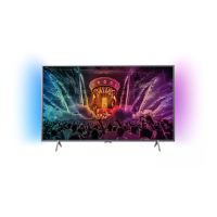
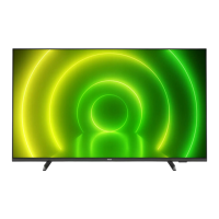
Do you have a question about the Philips 43PUT6801 and is the answer not in the manual?
Provides product information, getting started, FAQs, and software.
Directions for use can be downloaded from the following websites.
Details rear and side connections, including diagrams and pinouts.
Refers to Block Diagrams for PWB/CBA locations.
Safety regulations to follow during and after a repair, including transformer use and component checks.
Cautionary advice regarding electrostatic discharge (ESD), high voltage, and working with powered units.
General notes on measuring voltages/waveforms and schematic conventions.
Guidance on board exchange versus component-level repair and returning defective boards.
Precautions against electrical shock and handling of components.
List of abbreviations used in the manual, with their meanings.
Illustrates cable routing for various 6801 series models.
Describes the correct orientation and surface for safe TV servicing.
Step-by-step instructions for removing the stand bracket and rear cover.
Instructions for removing the stand bracket and rear cover for 6801 series models.
Steps for removing the rear cover and related components.
Procedures for reassembling the TV set, emphasizing cable placement and EMC foams.
Overview of Service Alignment Mode (SAM), Factory Mode, and Customer Service Mode (CSM).
Diagram illustrating the TV's power-on sequence states.
Information on ComPair tool and its usage.
Procedure for upgrading TV software via USB, including preparation and download steps.
Explanation of error codes, their meanings, and how they are displayed.
Method for displaying errors via front LED blinking when OSD is not working.
General tips for troubleshooting, NVM editing, and handling specific issues like no picture or audio.
Conditions required for performing electrical adjustments, including power supply and probe specifications.
Indicates that hardware alignments are not applicable.
Procedure for software alignments, including white point and display adjustments in SAM mode.
Information on option codes, how they are set in SAM, and their purpose.
Instructions for resetting NVM on a repaired SSB, including MAC address reload.
Defines the chassis cable position numbering rule starting with 'E'.
Overview of the QM16.3A LA chassis, its platform, and supported stylings.
Details the power supply unit architecture and diversity based on displays.
Lists DC/DC converter output voltages for various set executions.
Describes the front-end components for DVB-C and DTV parts.
Details HDMI input configurations and connector usage.
Explains the features of the MT5593UGIJ processor for video and audio.
Internal block diagram and pin configuration for the SOC-EMMC, MT5593UGIJ.
Block diagram of the 7101/7601 series, showing MT5593U and NT72324 connections.
Block diagram for the 6801 series, detailing MT5593U, NT72333, and other components.
Schematic for the AC input section of the 715G7831 PSU.
Schematic for the Power Factor Correction (PFC) stage using LD7591T.
Circuit diagram for the flyback converter section using SSC3S121.
Schematic for the LLC resonant converter stage using TPV101.
Top view layout of the power supply board.
Bottom view layout of the power supply board.
Schematic for the AC input section of the 715G7732 PSU.
Schematic for the Power Factor Correction (PFC) stage using TI components.
Circuit diagram for the flyback converter section using Sanken QR.
Schematic for the LLC resonant converter stage using Sanker components.
Top view layout of the 715G6679 power supply board.
Bottom view layout of the 715G6679 power supply board.
Schematic for the AC input section of the 715G7854 PSU.
Diagrams of various jumper configurations on the PCB.
Top view layout of the 715G7854 PSU board.
Bottom view layout of the 715G7854 PSU board.
Schematic for the AC input section of the 715G6679 PSU.
Schematic for the Power Factor Correction (PFC) circuit.
Schematic for the main power supply unit, including various converters and control ICs.
Schematic for the LED driver circuit, detailing components and connections.
Top view layout of the 715G6679 power supply board.
Bottom view layout of the 715G6679 power supply board.
Schematic for the AC input section of the 715G6677 PSU.
Schematic for the Power Factor Correction (PFC) circuit.
Schematic for the standby power supply circuit, including control ICs and protection.
Schematic for the LED driver circuit, detailing components and connections.
Top view layout of the 715G6677 power supply board.
Bottom view layout of the 715G6677 power supply board.
Schematic for the AC input section of the 715G6973 PSU.
Schematic for the Power Factor Correction (PFC) circuit.
Schematic for the main power supply unit, including converters and control ICs.
Schematic for the LED driver circuit, detailing components and connections.
Top view layout of the 715G6973 power supply board.
Bottom view layout of the 715G6973 power supply board.
Schematic for the AC input section of the 715G7720 PSU.
Schematic for the Power Factor Correction (PFC) circuit using LD7591T.
Schematic for the main power supply unit using SSC3S121A.
Schematic for the LED driver circuit, detailing components and connections.
Top view layout of the 715G7720 power supply board.
Bottom view layout of the 715G7720 power supply board.
Schematic for the AC input section of the 715G6679 PSU.
Schematic for the Power Factor Correction (PFC) circuit.
Schematic for the main power supply unit using SSC3S121A.
Schematic for the LED driver circuit, detailing components and connections.
Top view layout of the 715G6679 power supply board.
Bottom view layout of the 715G6679 power supply board.
Internal block diagram and pin configuration for the SOC-EMMC.
Schematic showing the DDR3 memory interface connections.
Schematic detailing DDR3 memory interface connections.
Schematic illustrating DDR3 memory interface connections.
Schematic for the front-end tuner and demodulator.
Schematic for the NT324a-Vx1 input interface.
Schematic showing General Purpose Input/Output (GPIO) connections.
Schematic illustrating the TX-VB1 interface.
Schematic for the power supply circuit.
Schematic showing the DDR memory interface connections.
Schematic detailing the ground connections for the NT72333.
Schematic for the system power DC/DC converters.
Schematic for DC/DC converters powering the SOC VCCK and DVSS.
Schematic for the system power DC/DC converters.
Internal block diagram and pin configuration for the SOC-EMMC.
Internal block diagram and pin configuration for the SOC-EMMC.
Schematic for LED drivers covering 49 to 64 LEDs.
Schematic for the NT324a-Vx1 input interface.
Schematics for HDMI inputs, detailing connectors and signal routing.
Schematic illustrating HDMI connections with Audio Return Channel (ARC).
Schematic for SCART, YPbPr, and CVBS input/output connections.
Schematic for control connectors, including IR receiver and Ethernet PHY.
Schematic for Ethernet PHY and related control circuitry.
Schematics for IR receiver, 3D, light sensor, and LOGO circuits.
Layout diagrams for the IR/LED board (top and bottom sides).
Schematics for IR receiver, 3D, light sensor, and LOGO circuits.
Layout diagrams for the IR/LED board (top and bottom sides).
Schematics for the IR receiver, light sensor, and standby LED circuits.
Layout diagrams for the IR/LED board (top and bottom sides).
Schematic for the KEY+AL section, including joystick circuit.
Layout diagrams for the keyboard control panel (top and bottom sides).
Schematic for the key input section with joystick circuit.
Layout diagrams for the keyboard control panel (top and bottom sides).
Schematic for the LED LOGO circuit, showing LED drivers and connections.
Layout diagrams for the LED board (top and bottom sides).
Schematic for the Ambilight board with TLC5971 driver IC.
Layout diagrams for the Ambilight board (top and bottom sides).
Schematic for the Ambilight board with TCL5971 driver IC.
Schematic for the Ambilight board with TCL5971 driver IC.
Schematic for the 6-LED Ambilight array.
Schematic for the 7-LED Ambilight array.
Layout diagrams for the Ambilight board (top and bottom sides).
Exploded view and parts list for the 43-inch 6801 series TV.
Exploded view and parts list for the 49-inch 6801 series TV.
Exploded view and parts list for the 55-inch 6801 series TV.
Exploded view and parts list for the 55-inch 7101 series TV.
Exploded view and parts list for the 65-inch 7101 series TV.
Exploded view and parts list for the 65-inch 7601 series TV.
Exploded view and parts list for the 75-inch 7101 series TV.


