LTE-A Module Series
EM120R-GL&EM160R-GL Hardware Design
EM120R-GL&EM160R-GL_Hardware_Design 47 / 79
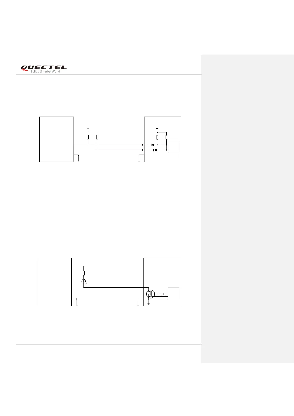
A simple level shifter based on diodes is used on W_DISABLE1# pin and W_DISABLE2# pin which are
pulled up to a 1.8 V voltage in the module, as shown in the following figure. So, the control signals (GPIO)
of the host device could be a 1.8 V or 3.3 V voltage level and pull-up resistor is not needed on the host
side. These two signals are active low, and a reference circuit is shown below.
Host Module
W_DISABLE2#
W_DISABLE1#
BB
GPIO
GPIO
26
8
VDD 1.8 V
Note:
Host’s GPIO could be a 1.8 V or 3.3 V voltage level.
R2
10K
R1
10K
VCC_IO_HOST
R4
10K
R3
10K
Figure 27: W_DISABLE1# and W_DISABLE2# Reference Circuit
3.10.3. WWAN_LED# Signal
The WWAN_LED# signal is used to indicate RF status of the modules, and its typical current
consumption is up to 10 mA.
In order to reduce the current consumption of the LED, a resistor must be placed in series with the LED,
as illustrated in the figure below. The LED is ON when the WWAN_LED# signal is at a low voltage level.
Host Module
WWAN_LED#
PMU
GPIO
10
VCC
Note: This VCC could be the power supply of the module.
LED
R1
200Ω
Figure 28: WWAN_LED# Signal Reference Circuit