LTE-A Module Series
EM120R-GL&EM160R-GL Hardware Design
EM120R-GL&EM160R-GL_Hardware_Design 23 / 79
3.3. Power Supply
The following table shows definition of VCC pins and ground pins.
Table 4: Pin Definition of VCC and GND
3.3.1. Decrease Voltage Drop
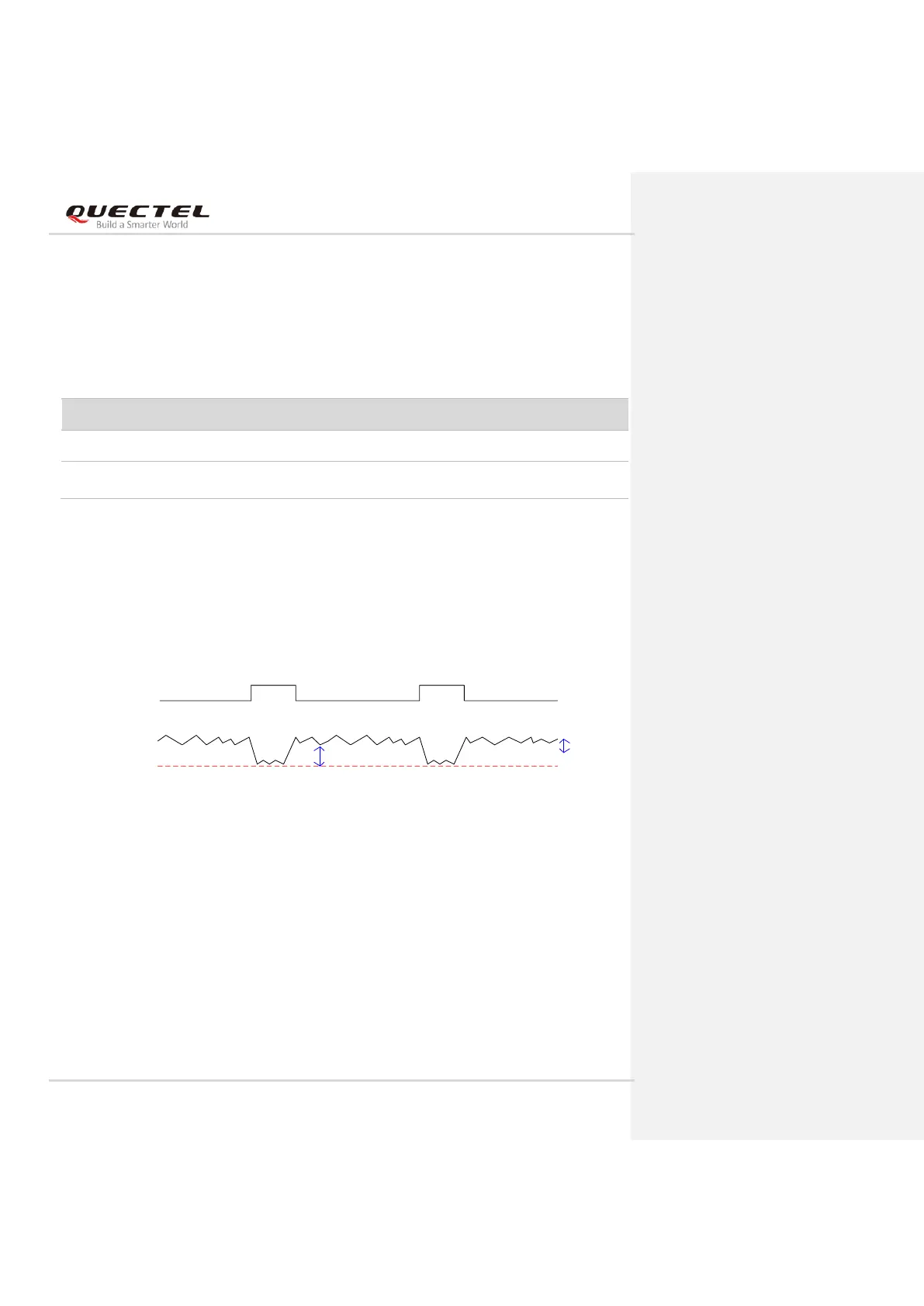
The power supply range of the module is from 3.135 V to 4.4 V. Make sure that the input voltage never
drops below 3.135 V, otherwise the module will be powered off automatically. The following figure shows
the maximum voltage drop during radio transmission in 3G and 4G networks.
Figure 3: Power Supply Limits during Radio Transmission
To decrease voltage drop, a bypass capacitor of about 220 µF with low ESR (ESR = 0.7 Ω) should be
used, and a multi-layer ceramic chip capacitor (MLCC) array should also be reserved due to its ultra-low
ESR. It is recommended to use three ceramic capacitors (100 nF, 33 pF, 10 pF) for composing the MLCC
array, and place these capacitors close to VCC pins. The main power supply from an external application
must be a single voltage source. The width of VCC trace should be no less than 2 mm. In principle, a
longer VCC trace indicates a wider VCC trace.
In addition, in order to get a stable power source, it is recommended to use a zener diode with reverse
zener voltage of 5.1 V and dissipation power more than 0.5 W. The following figure shows a reference
3, 5, 11, 27, 33, 39, 45,
51, 57, 71, 73